Table 4-11. gpsr2 register bitmap, Table 4-12. gpcr0 bit definitions, Table 4-13. gpcr1 bit definitions – Intel PXA26X User Manual
Page 120: Table 4-11, Table 4-12, Table 4-13
4-12
Intel® PXA26x Processor Family Developer’s Manual
System Integration Unit
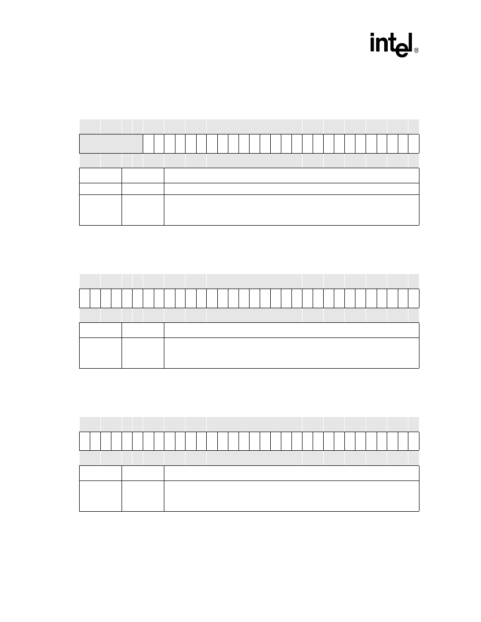
Table 4-11. GPSR2 Register Bitmap
Physical Address
0x40E0_0020
GPIO Pin Output Set Register2
(GPSR2)
System Integration Unit
Bit
31 30 29 28 27 26 25 24 23 22 21 20 19 18 17 16 15 14 13 12 11 10 9
8
7
6
5
4
3
2
1
0
Reserved
PS8
9
PS8
8
PS8
7
PS8
6
PS8
5
PS8
4
PS8
3
PS8
2
PS8
1
PS8
0
PS7
9
PS7
8
PS7
7
PS7
6
PS7
5
PS7
4
PS7
3
PS7
2
PS7
1
PS7
0
PS6
9
PS6
8
PS6
7
PS6
6
PS6
5
PS6
4
Reset
0
0
0
0
0
0
0
0
0
0
0
0
0
0
0
0
0
0
0
0
0
0
0
0
0
0
0
0
0
0
0
0
Bits
Name
Description
<31:26>
—
Reserved
<25:0>
PS[x]
GPIO Pin ‘x’ Output Pin Set (where x = 64 through 89).
0 – Pin level unaffected.
1 – If pin configured as an output, set pin level high (one).
Table 4-12. GPCR0 Bit Definitions
Physical Address
0x40E0_0024
GPCR0
System Integration Unit
Bit
31 30 29 28 27 26 25 24 23 22 21 20 19 18 17 16 15 14 13 12 11 10 9
8
7
6
5
4
3
2
1
0
PC
3
1
PC
3
0
PC
2
9
PC
2
8
PC
2
7
PC
2
6
PC
2
5
PC
2
4
PC
2
3
PC
2
2
PC
2
1
PC
2
0
PC
1
9
PC
1
8
PC
1
7
PC
1
6
PC
1
5
PC
1
4
PC
1
3
PC
1
2
PC
1
1
PC
1
0
PC
9
PC
8
PC
7
PC
6
PC
5
PC
4
PC
3
PC
2
PC
1
PC
0
Reset
0
0
0
0
0
0
0
0
0
0
0
0
0
0
0
0
0
0
0
0
0
0
0
0
0
0
0
0
0
0
0
0
Bits
Name
Description
<31:0>
PC[x]
GPIO Pin ‘x’ Output Pin Clear (where x = 0 through 31).
0 – Pin level unaffected.
1 – If pin configured as an output, clear pin level low (zero).
Table 4-13. GPCR1 Bit Definitions
Physical Address
0x40E0_0028
GPCR1
System Integration Unit
Bit
31 30 29 28 27 26 25 24 23 22 21 20 19 18 17 16 15 14 13 12 11 10 9
8
7
6
5
4
3
2
1
0
PC6
3
PC6
2
PC6
1
PC6
0
PC5
9
PC5
8
PC5
7
PC5
6
PC5
5
PC5
4
PC5
3
PC5
2
PC5
1
PC5
0
PC4
9
PC4
8
PC4
7
PC4
6
PC4
5
PC4
4
PC4
3
PC4
2
PC4
1
PC4
0
PC3
9
PC3
8
PC3
7
PC3
6
PC3
5
PC3
4
PC3
3
PC3
2
Reset
0
0
0
0
0
0
0
0
0
0
0
0
0
0
0
0
0
0
0
0
0
0
0
0
0
0
0
0
0
0
0
0
Bits
Name
Description
<31:0>
PC[x]
GPIO Pin ‘x’ Output Pin Clear (where x = 32 through 63).
0 – Pin level unaffected.
1 – If pin configured as an output, clear pin level low (zero).