5 configuring the intel strataflash® memory, Table 18-1 – Intel PXA26X User Manual
Page 619
Intel® PXA26x Processor Family Developer’s Manual
18-3
Internal Flash
Warning:
Using a memory-clock frequency above 133 MHz is not allowed in synchronous mode with Intel
StrataFlash® memory.
18.1.5
Configuring the Intel StrataFlash® Memory
To configure the Intel StrataFlash® memory for synchronous operation, software must write the
RCR inside the Intel StrataFlash® memory. The RCR value is written over the address lines.
Because the 16- and 32-bit versions of the PXA26x processor family have address lines connected
differently, the address used to set the RCR settings for each is different. Also, since the 256/16
version has two memory chips the RCR value has to be written to two addresses.
As per the Intel StrataFlash® memory specification, the RCR value is written twice. The first write
data must be 0x60. The second write data must be 0x03. After the RCR write procedure is
completed, the memory defaults to read-array mode.
See
for information on values to program and addresses.
Warning:
The CAS latency setting within SXCNFG[SXCLx] is one less than the actual setting. For example,
setting SXCNFG[SXCLx]=0b100 gives a CAS latency of 5 clocks. The CAS latency value
programmed into the flash is also one less than the actual setting.
Note:
The instructions to do the RCR configuration sequence and the SXCNFG above must either be in
RAM or guaranteed not to fetch from the flash during the RCR write/SXCNFG operation. This is
accomplished by placing the write instructions on a cache line boundary followed by a branch,
since the PXA26x processor family processor always fetches eight instructions at a time, even with
the instruction cache off, and the branch forces the pre-fetcher to flush the pipeline, preventing a
fetch until the processor and flash have both reached synchronous mode.
This code correctly configures the flash into synchronous mode depending on the bus width,
frequency, and size:
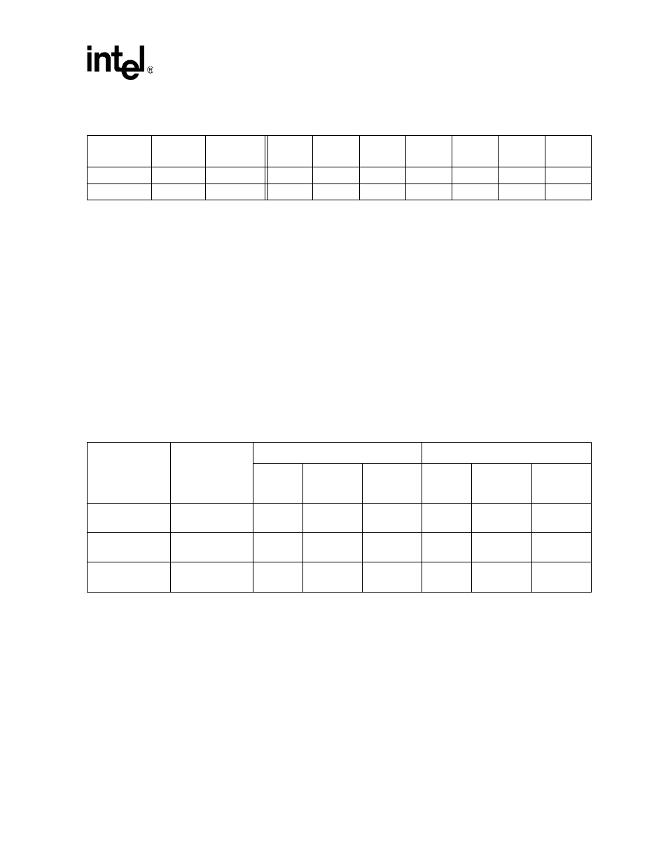
Table 18-1. SXCNFG Configuration for Internal Flash
Memory Clock
Frequency
SDCLK[0]
Frequency
SXCNFG
SXLATCH
0
SXTP0
SXCA0
SXRA0
SXRL0
SXCL0
SXEN0
100 MHz
50 MHz
0xXXXX 60F1
1
0b10
0
0
0b111
0b100
0b01
133 MHz
66 MHz
0xXXXX 60F9
1
0b10
0
0
0b111
0b110
0b01
Table 18-2. RCR Values for Each PXA26x processor family Applications Processor Version
PXA26x Processor
Family Version
Flash Width
100-MHz-Memory Clock
133-MHz-Memory Clock
RCR
Register
Setting
Address to
Write
1st Data
2nd Data
RCR
Register
Setting
Address to
Write
1st Data
2ndData
PXA261 processor
128 Mbit
16-Bits Wide
0x25C2
0x4B84
0x0060
0x0003
0x35C2
0x6B84
0x0060
0x0003
PXA262 processor
256 Mbit
16-Bits Wide
0x25C2
0x4B84
0x0100 4B84
0x0060
0x0003
0x35C2
0x6B84
0x0100 6B84
0x0060
0x0003
PXA263 processor
256 Mbit
32-Bits Wide
0x25C2
0x9708
0x0060 0060
0x0003 0003
0x35C2
0xD708
0x0060 0060
0x0003 0003