Intel PXA26X User Manual
Page 580

16-32
Intel® PXA26x Processor Family Developer’s Manual
Network/Audio Synchronous Serial Protocol Serial Ports
15:12
R
RFL
RECEIVE FIFO LEVEL:
The number of valid entries (minus 1) currently in the receive FIFO.
When the value of 0xF is read, the FIFO is either empty or full and
programmers must refer to RNE.
11:8
R
TFL
TRANSMIT FIFO LEVEL:
Number of valid entries (minus 1) currently in the transmit FIFO.
When the value of 0x0 is read, the FIFO is either empty or full and
programmers must refer to TNF.
7
R/W
ROR
RECEIVE FIFO OVERRUN:
Indicates that the Receive logic attempted to place data into the receive
FIFO after it had been completely filled. When new data is received,
ROR is asserted and the newly received data is discarded. This
process is repeated for all new data received until at least one empty
FIFO entry exists.
When set, an interrupt is generated to the CPU that cannot be locally
masked by any SSP port register bit. The setting of ROR does not
generate any DMA service request. Clearing this bit resets its interrupt
request.
Write one to clear this bit.
0 – Receive FIFO has not experienced an overrun
1 – Attempted data write to full receive FIFO, request Interrupt
6
R
RFS
RECEIVE FIFO SERVICE REQUEST:
Indicates that the receive FIFO requires service to prevent an overrun.
RFS is set when the number of valid entries in the receive FIFO is equal
to or greater than the receive FIFO trigger threshold. It is cleared when
it has fewer entries than the trigger threshold value. When RFS is set,
an Interrupt is generated when SSCR1[RIE] is set. Setting RFS signals
a DMA service request if SSCR1[RSRE] is set. After the CPU or DMA
reads the FIFO such that it has fewer entries than the value of
SSCR1[RFT], RFS (and the service request or interrupt) is
automatically cleared. SSCR1[RSRE] and SSCR1[RIE] must not both
be set.
0 – Receive FIFO level exceeds RFT trigger threshold or the SSP port
is disabled
1 – Receive FIFO level is at or above RFT trigger threshold, request
Interrupt
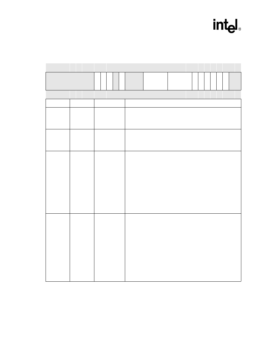
Table 16-8.
SSSR Bit Definitions (Sheet 2 of 3)
Physical Address
Base + 0x08
SSSR
PXA26x processor family Network/Audio
SSP Serial Ports
Bit
31 30 29 28 27 26 25 24 23 22 21 20 19 18 17 16 15 14 13 12 11 10 9
8
7
6
5
4
3
2
1
0
Reserved
BC
E
CS
S
TU
R
R
eser
ved
TIN
T
R
eser
ved
RF
L
TF
L
RO
R
RF
S
TFS
BS
Y
RN
E
TN
F
R
eser
ved
Reset
?
?
?
?
?
?
?
?
0
0
0
?
0
?
?
?
1
1
1
1
0
0
0
0
0
0
0
0
0
1
?
?
Bits
Access
Name
Description
