14 memory map – Intel PXA26X User Manual
Page 63
Intel® PXA26x Processor Family Developer’s Manual
2-33
System Architecture
2.14
Memory Map
and
show the full processor memory map.
Any unused register space from 0x4000 0000 to 0x4BFF FFFF is reserved.
Note:
Accessing reserved portions of the memory map gives unpredictable results.
The PCMCIA interface is divided into socket 0 and socket 1 space. These two partitions are each
subdivided into I/O, memory and attribute space. Each is allocated 128 MB of memory space.
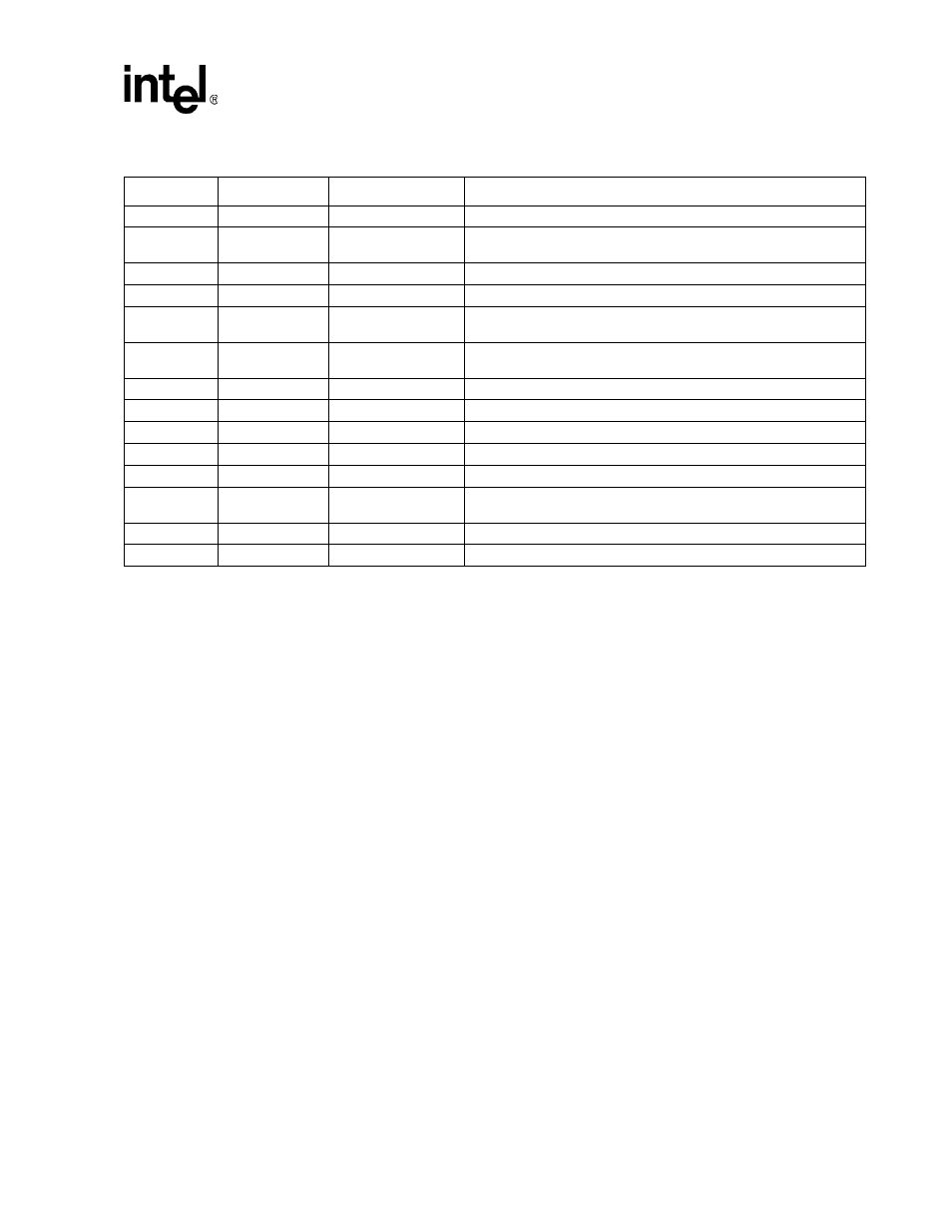
0x4800 0010
MSC2
Static Memory Control Register 2
0x4800 0014
MECR
Expansion Memory (PCMCIA/Compact Flash) Bus Configuration
Register
0x4800 001C
SXCNFG
Synchronous Static Memory Control Register
0x4800 0024
SXMRS
MRS value to be written to SMROM
0x4800 0028
MCMEM0
Card interface Common Memory Space Socket 0 Timing
Configuration
0x4800 002C
MCMEM1
Card interface Common Memory Space Socket 1 Timing
Configuration
0x4800 0030
MCATT0
Card interface Attribute Space Socket 0 Timing Configuration
0x4800 0034
MCATT1
Card interface Attribute Space Socket 1 Timing Configuration
0x4800 0038
MCIO0
Card interface I/O Space Socket 0 Timing Configuration
0x4800 003C
MCIO1
Card interface I/O Space Socket 1 Timing Configuration
0x4800 0040
MDMRS
MRS value to be written to SDRAM
0x4800 0044
BOOT_DEF
Read-Only Boot-Time Register. Contains BOOT_SEL and PKG_SEL
values.
0x4800 0058
MDMRSLP
Low-Power SDRAM Mode Register Set Configuration Register
0x4800 0064
SA1111CR
SA1111 compatibility register
Table 2-8. Register Address Summary (Sheet 13 of 13)
Unit
Address
Register Symbol
Register Description