1 non-sdram timing flash read timing diagram – Intel PXA26X User Manual
Page 230
6-40
Intel® PXA26x Processor Family Developer’s Manual
Memory Controller
6.7.4.1
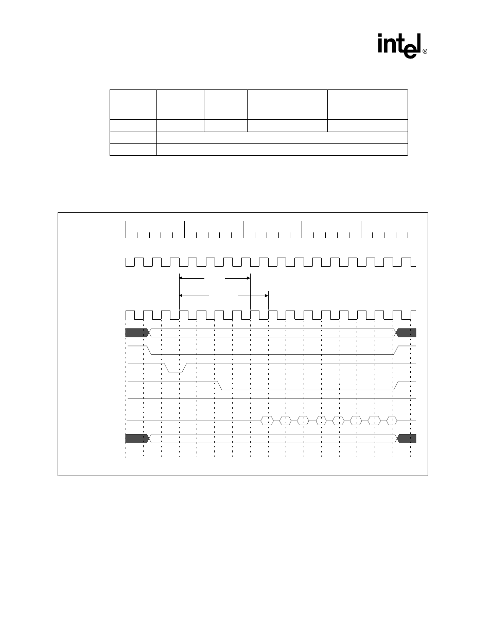
Non-SDRAM Timing Flash Read Timing Diagram
The burst-of-eight read timing diagram is shown in
.
In
, the following timing parameters apply:
•
nADV asserted time = 1 MEMCLK
•
MA, nCS setup to nADV asserted = 1 MEMCLK
•
nADV deasserted to nOE asserted = Code – 2 MEMCLKs
For divide-by-two mode, the following timing parameters apply:
133
66
1
5 / 6
6 / 7
147
Not supported
166
Not supported
Table 6-19. Frequency Code Configuration Values Based on Clock Speed (Sheet 2 of 2)
MEMCLK
Frequency
SDCLK0
Frequency
MDREFR:
K0DB2
Valid
Frequency
Configurations
Corresponding
CAS Latencies
Figure 6-12. Burst-of-Eight Synchronous Flash Timing Diagram (non-divide-by-2 mode)
addr
0000
CODE+1
CODE
CODE+1
This diagram is for SXCNFG:CL = 0b100, CAS latency = 5
memclk
SDCLK[0]
MA[19:0]
nCS[0/1/2/3]
nADV(nSDCAS)
nOE
nWE
MD
DQM[3:0]