4 examples – Intel PXA26X User Manual
Page 183
Intel® PXA26x Processor Family Developer’s Manual
5-25
Direct Memory Access Controller
5.4
Examples
This section contains examples that show how to:
•
Set up and start a channel
•
Initialize a descriptor list for a channel that is running
•
Add a descriptor to the end of a descriptor list for a channel that is running
•
Initialize a channel that is going to be used by a direct DMA master
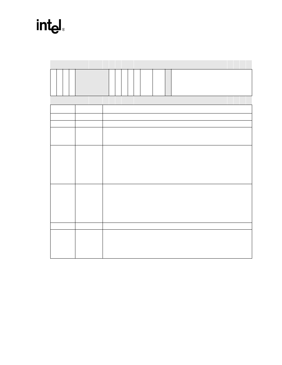
20
—
Reserved – Read as unknown and must be written as zero.
19
—
Reserved – Read as unknown and must be written as zero.
18
ENDIAN
DEVICE ENDIAN-NESS (read / write):
0 – Byte ordering is little endian
1 – Reserved
17:16
SIZE
MAXIMUM BURST SIZE – Of each data transferred (read / write):
00 – Reserved
01 – 8 Bytes
10 – 16 Bytes
11 – 32 Bytes
If DCMDx[LENGTH] is less than DCMDx[SIZE] the data transfer size equals
DCMDx[LENGTH].
15:14
WIDTH
WIDTH OF THE ON-CHIP PERIPHERAL (read / write/):
00 – Reserved
01 – 1 byte
10 – HalfWord (2 bytes)
11 – Word (4 Bytes)
Must be programmed 00 for memory-to-memory moves or companion-chip related
operations.
13
—
Reserved – Read as unknown and must be written as zero
12:0
LENGTH
LENGTH OF TRANSFER IN BYTES (read / write):
Indicates the length of transfer in bytes. DCMD[LENGTH] = 0 means zero bytes for
Descriptor Fetch Mode only. DCMD[LENGTH] = 0 is an invalid setting for the No-Descriptor
Fetch Mode. The maximum transfer length is (8K-1) bytes. If the transfer involves any of
the internal peripherals, the length of the transfer must be an integer multiple of the width of
that peripheral.
Table 5-12. DCMDx Register Bitmap and Bit Definitions (Sheet 2 of 2)
0x4000_02xC
DMA Command Register (DCMDx)
DMAC
Bit
31 30 29 28 27 26 25 24 23 22 21 20 19 18 17 16 15 14 13 12 11 10 9
8
7
6
5
4
3
2
1
0
IN
CS
RC
AD
DR
IN
CT
R
G
AD
DR
FLO
WSR
C
FLO
WTR
G
R
ESE
RVED
S
T
AR
T
IRQ
EN
EN
DI
R
Q
E
N
R
ESE
RVED
R
ESE
RVED
EN
DIA
N
SIZE
WID
T
H
R
ESE
RVED
LE
N
G
T
H
Reset
0
0
0
0
0
0
0
0
0
0
0
0
0
0
0
0
0
0
0
0
0
0
0
0
0
0
0
0
0
0
0
0
Bits
Name
Description