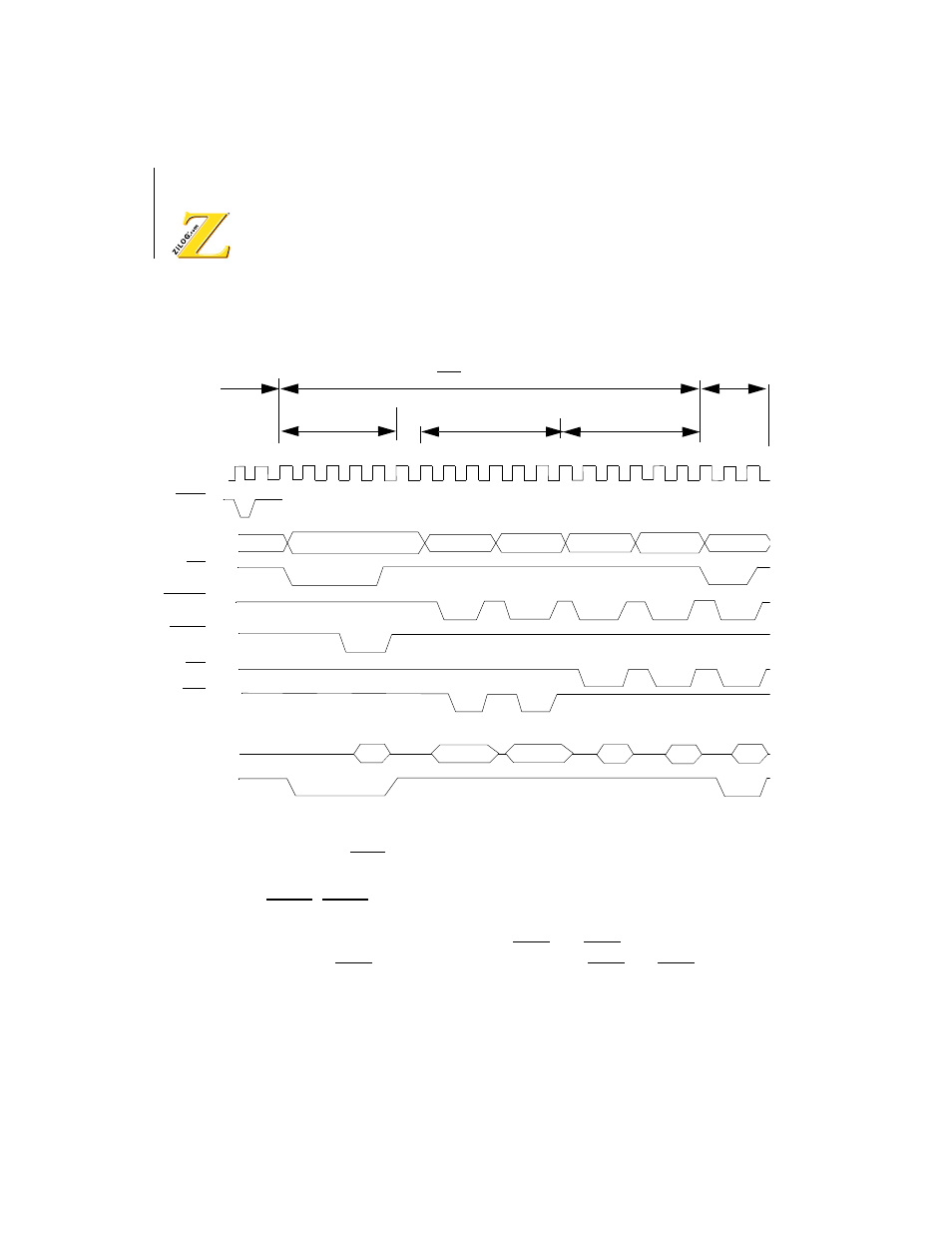
Figure 40. int0 interrupt mode 2 timing diagram, Int1, int2 – Zilog Z80180 User Manual
Page 95

Z8018x
Family MPU User Manual
80
UM005003-0703
Figure 40. INT0 Interrupt Mode 2 Timing Diagram
INT1, INT2
The operation of external interrupts INT1 and INT2 is a vector mode
similar to INT0 Mode 2. The difference is that INT1 and INT2 generate
the low-order byte of vector table address using the IL (Interrupt Vector
Low) register rather than fetching it from the data bus. This difference is
A0
–
A19
WR
RD
MREQ
D0
–
D7
M1
PC
SP-1
SP-2
INT0
T1
T3
TW*
T2
Ti
T2
T1
T3
T1
T2 T3
TW*
*Two Wait States are automatically inserted
ST
IORQ
Vector
Vector+1
Vector Lower
Address Read
PC is pushed onto stack
Interrupt
Op Code
T1
T1
T1
T2 T3
T2
T2
T3
Starting address
PCH
PCL
Starting Address
Starting Address
(Upper Address)
(Lower Address)
Lower Vector
Phi
Manipulation
Cycle
Fetch Cycle
INT0 Acknowledge Cycle
Last MC
