Table 4, Wait state insertion – Zilog Z80180 User Manual
Page 45
Z8018x
Family MPU User Manual
30
UM005003-0703
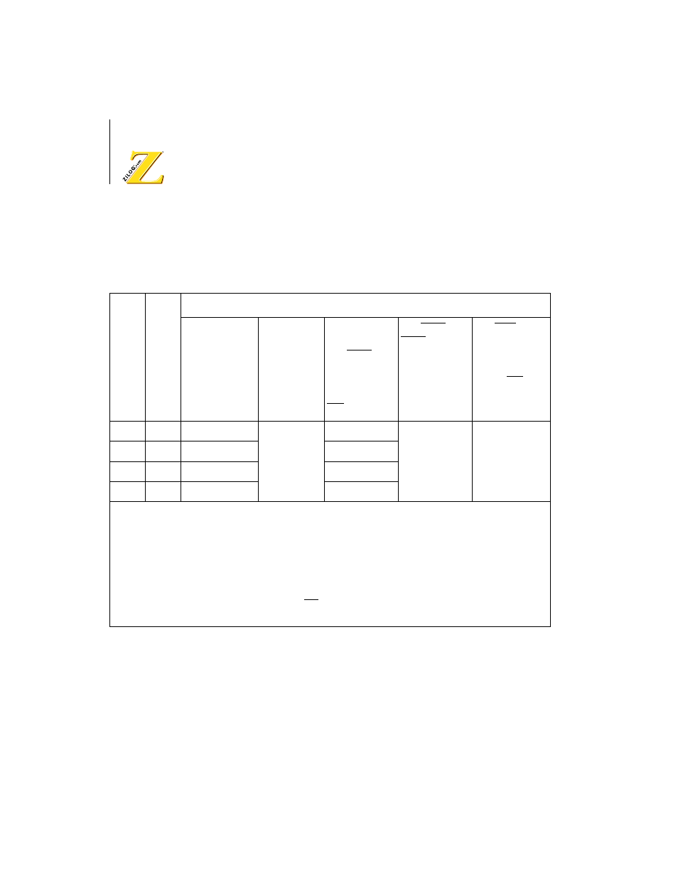
inserted depending on the programmed value in IWI1 and IWI0. Refer to
Table 4.
WAIT Input and RESET
During RESET, MWI1, MWI0 IWI1 and IWI0, are all
1
, selecting the
maximum number of Wait States (TW) (three for memory accesses, four
for external I/O accesses).
Table 4.
Wait State Insertion
IWI1 IWI0
The Number of Wait States
For external
I/O registers
accesses
For internal
I/0
registers
accesses
For INT0
interrupt
acknowledge
cycles when
M1 is Low
For INT1,
INT2 and
internal
interrupts
acknowledge
cycles
(Note 2)
For NMI
interrupt
acknowledge
cycles
when M1 is
Low
(Note 2)
0
0
1
0
(Note 1)
2
2
0
0
1
2
4
1
0
3
5
1
1
4
6
Note:
1.
For Z8X180 internal I/O register access (I/O addresses
0000H
-
003FH
), IWI1 and IWI0 do not
determine wait state (TW) timing. For ASCI, CSI/O and PRT Data Register accesses, 0 to 4 Wait States
(TW) are generated. The number of Wait States inserted during access to these registers is a function of
internal synchronization requirements and CPU state. All other on-chip I/O register accesses (that is,
MMU, DMAC, ASCI Control Registers, for instance.) have no Wait States inserted and thus require only
three clock cycles.
2.
For interrupt acknowledge cycles in which M1 is High, such as interrupt vector table read and PC
stacking cycle, memory access timing applies.