Example of board design – Zilog Z80180 User Manual
Page 186

Z8018x
Family MPU User Manual
UM005003-0703
171
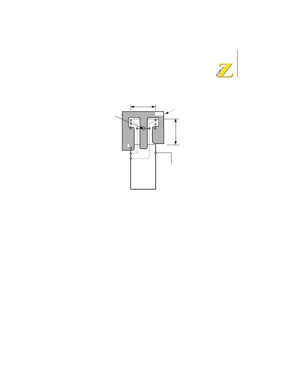
Figure 73. Example of Board Design
Circuit Board design should observe the following parameters.
•
Locate the crystal and load capacitors as close to the IC as physically
possible to reduce noise.
•
Signal lines must not run parallel to the clock oscillator inputs. In
particular, the clock input circuitry and the system clock output (pin 64)
must be separated as much as possible.
•
V
CC
power lines must be separated from the clock oscillator input
circuitry.
•
Resistivity between XTAL or EXTAL and the other pins must be
greater than 10M ohms.
Signal line layout must avoid areas marked with the shaded area of Figure
73.
Signal line layout must
avoid shaded areas
20 mm max
20 m
m
ma
x
Crystal
C
L
C
L
64
2
3
1
GND
Z8X180
Phi
Top View
Note: Pin mumbers valid only
for DIP configuration
