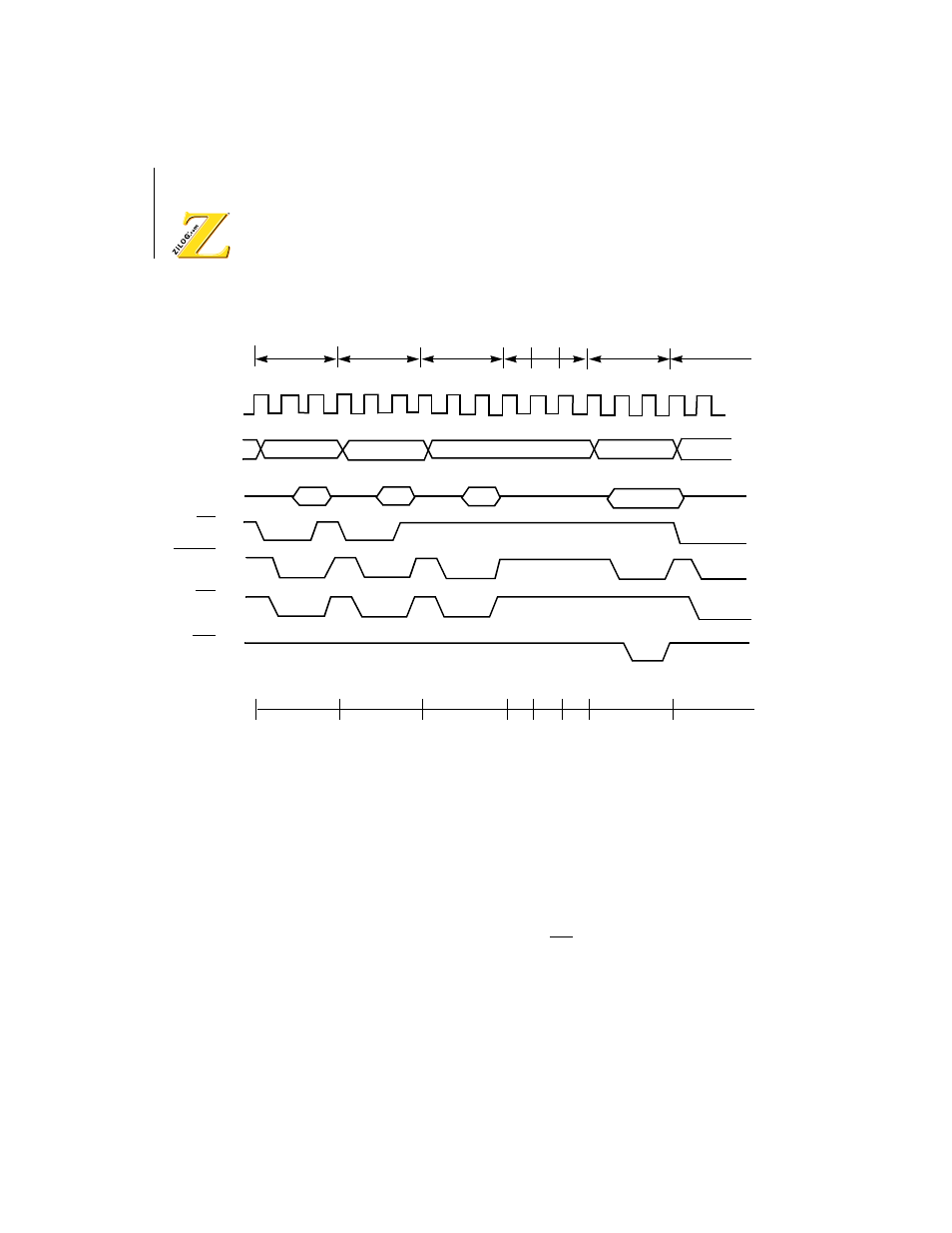
Figure 14. instruction timing diagram – Zilog Z80180 User Manual
Page 39

Z8018x
Family MPU User Manual
24
UM005003-0703
Figure 14. Instruction Timing Diagram
This instruction moves the contents of a CPU register (g) to the memory
location with address computed by adding a signed 8-bit displacement (d)
to the contents of an index register (IX).
The instruction cycle begins with the two machine cycles to read the two
byte instruction Op Code as indicated by M1 Low. Next, the instruction
operand (d) is fetched.
Memory
Write Cycle
Next instruction
Fetch Cycle
CPU internal
Operation
Displacement
Read Cycle
2nd Op Code
Fetch Cycle
1st Op Code
Fetch Cycle
T1 T2 T3 T1
T3 T1
T2
T2 T3 T1 T1 T1 T1
T1
T2 T3
T2
PC+3
IX+d
PC+2
PC+1
PC
g
(7OH
–
77H)
(DDH)
d
MC1
MC2
MC3
MC4 MC5 MC6
MC7
NOTE: d = displacement
g = register contents
Machine Cycle
WR
RD
MREQ
Phi
A0
–
A19
D0
–
D7
M1
