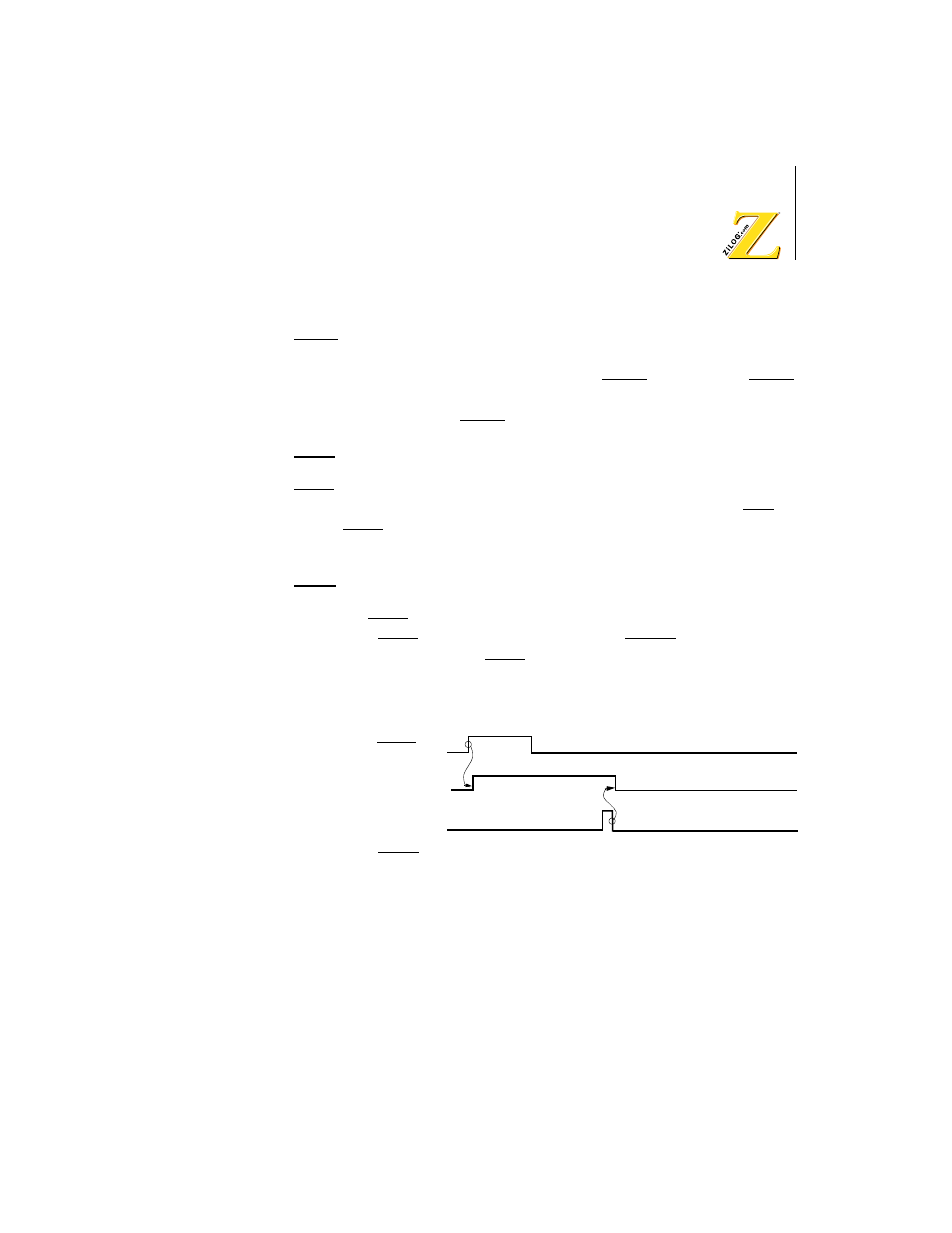
Figure 53. dcd0 timing diagram – Zilog Z80180 User Manual
Page 154

Z8018x
Family MPU User Manual
UM005003-0703
139
The error flags (PE, FE, and OVRN bits) are also held at
0
. Even after the
DCD0 input goes Low, these bits do not resume normal operation until
the status register (STAT0, is read. This first read of (STAT0, while
enabling normal operation, still indicates the DCD0 input is High (DCD0
bit = 1) even though it has gone Low. Thus, the STAT0 register must be
read twice to ensure the DCD0 bit is reset to
0
:
RTS0: Request to Send 0 (Output)
RTS0 allows the ASCI to control (start/stop) another communication
devices transmission (for example, by connection to that device's CTS
input). RTS0 is essentially a 1-bit output port, having no side effects on
other ASCI registers or flags.
CTS1: Clear to Send 1 (Input)
Channel 1 CTS1 input is multiplexed with Clocked Serial Receive Data
(RXS). The CTS1 function is selected when the CTS1E bit in STAT1 is
set to
1
. When enabled, the CTS1 operation is equivalent to CTS0,
Modem control signal timing is depicted in Figure 53 and Figure 54.
Figure 53. DCD0 Timing Diagram
DCD0 Pin
DCD0 Flag
Status Register Read
