Zilog Z80180 User Manual
Page 278
Z8018x
Family MPU User Manual
262
UM005003-0703
LD g, (IX+d)
LD g, (IY+d)
MC1
T1T2T3 1st Op Code
Address
1st Op
Code
0
1
0
1
0
1
0
MC2
T1T2T3 2nd Op Code
Address
2nd Op
Code
0
1
0
1
0
1
1
MC3
T1T2T3 1st operand
Address
d
0
1
0
1
1
1
1
MC4~M
C5
TiTi
*
Z
1
1
1
1
1
1
1
MC6
T1T2T3 IX+d
IY+d
DATA
0
1
0
1
1
1
1
LD (HL),g
MC1
T1T2T3 1st Op Code
Address
1st Op
Code
0
1
0
1
0
1
0
MC2
Ti
*
Z
1
1
1
1
1
1
1
MC3
T1T2T3 HL
g
1
0
0
1
1
1
1
LD (IX + d),g
LD (IY + d),g
MC1
T1T2T3 1st Op Code
Address
1st Op
Code
0
1
0
1
0
1
0
MC2
T1T2T3 2nd Op Code
Address
2nd Op
Code
0
1
0
1
0
1
1
MC3
T1T2T3 1st operand
Address
d
0
1
0
1
1
1
1
MC4~
MC6
TiTiTi *
Z
1
1
1
1
1
1
1
MC7
T1T2T3 IX+d
IY+d
g
1
0
0
1
1
1
1
LD (HL),m
MC1
T1T2T3 1st Op Code
Address
1st Op
Code
0
1
0
1
0
1
0
MC2
T1T2T3 1st operand
Address
m
0
1
0
1
1
1
1
MC3
T1T2T3 HL
DATA
1
0
0
1
1
1
1
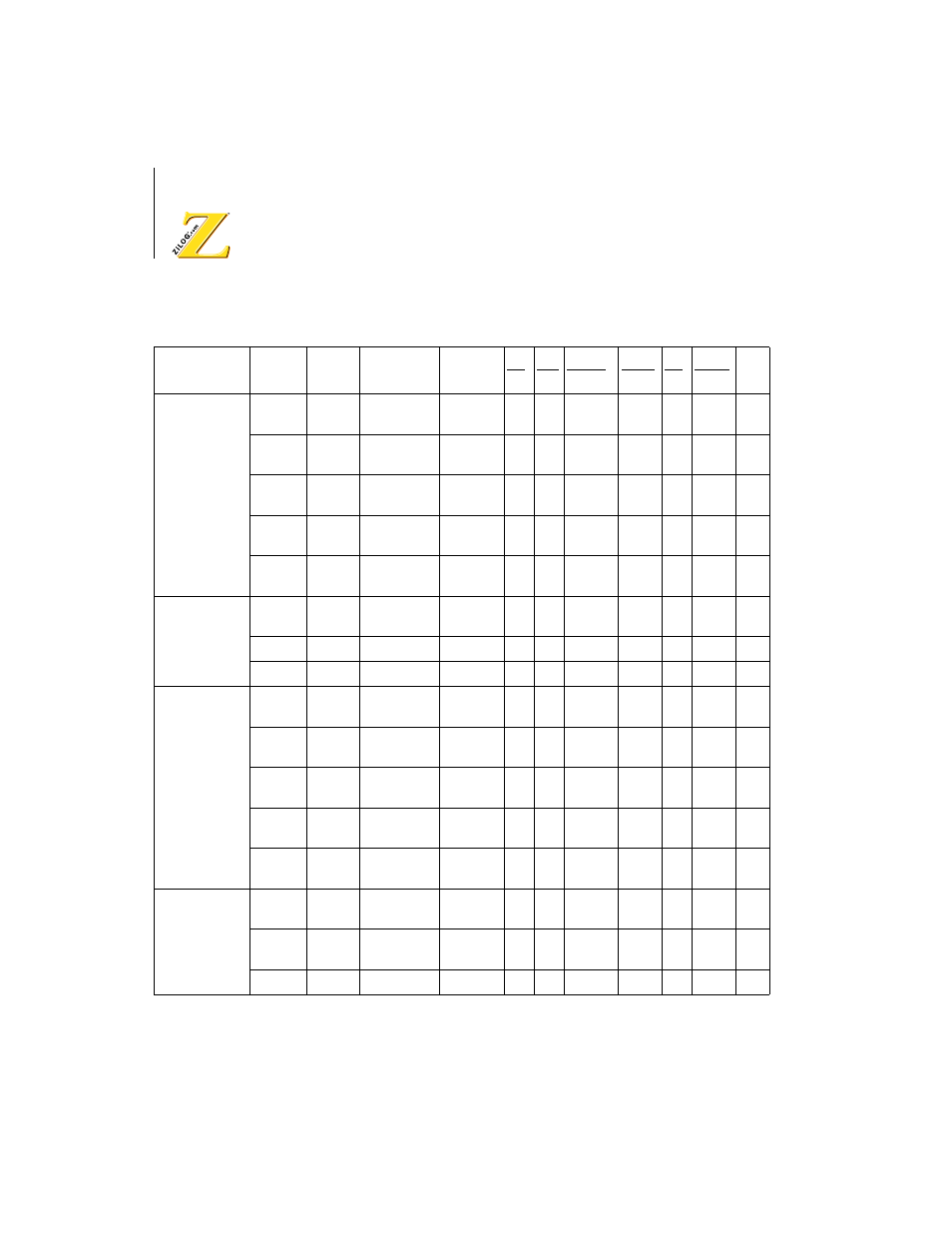
Table 51. Bus and Control Signal Condition in Each Machine Cycle (Continued)
Instruction
Machine
Cycle
States
Address
Data
RD WR MREQ
IORQ M1 HALT ST