Cpu operation and dma operation dreq0, Is programmed for edge-sense, Figure 49. tend0 output timing diagram – Zilog Z80180 User Manual
Page 123: Dma transfer (reference figure 49)
Z8018x
Family MPU User Manual
108
UM005003-0703
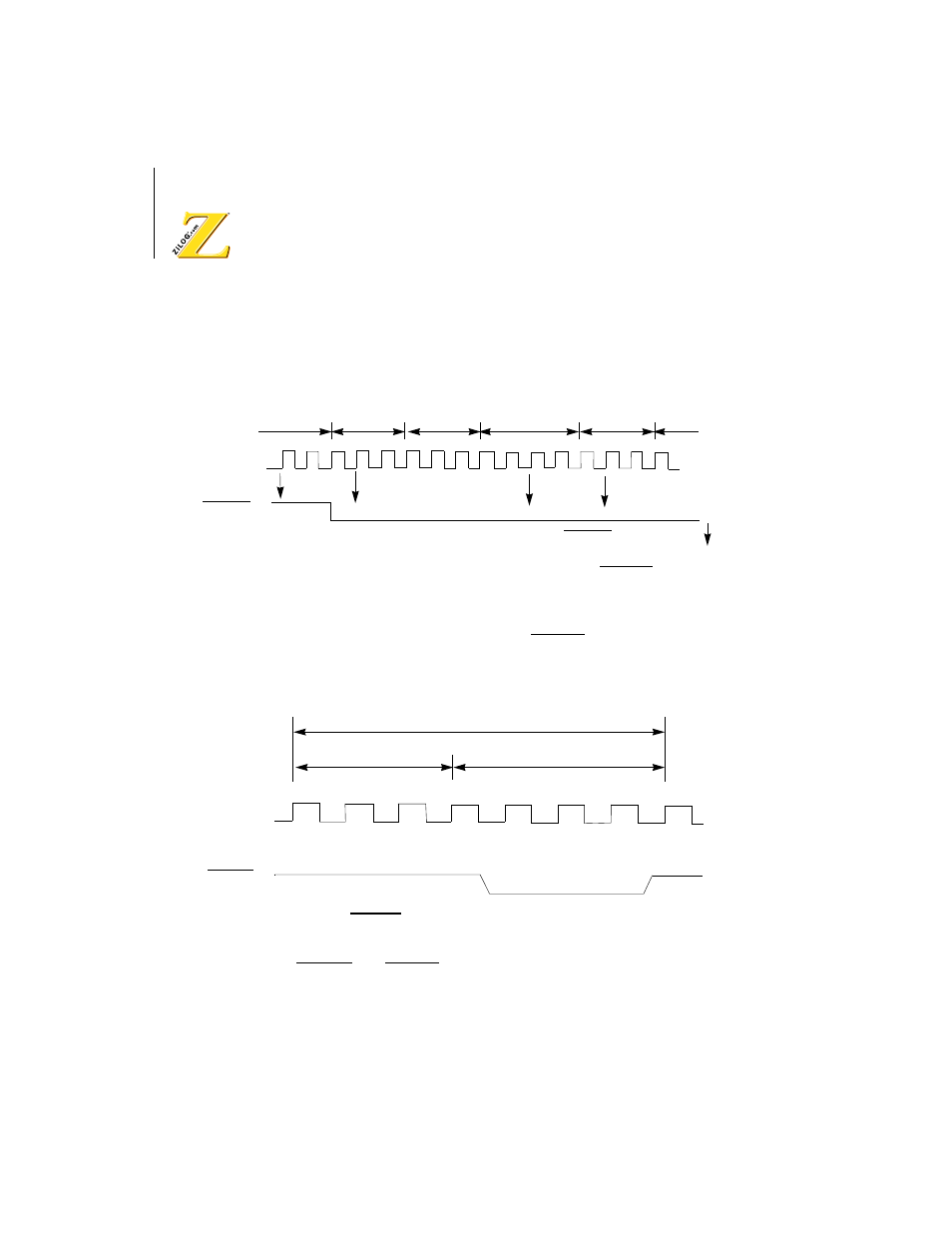
rising edge of the clock prior to T3 at which time the DMA operation
(re)starts. Figure 48 depicts the edge-sense DMA timing.
Figure 48. CPU Operation and DMA Operation DREQ0 is Programmed
for Edge-Sense
During the transfers for channel 0, the TEND0 output goes Low
synchronous with the write cycle of the last (BCR0 =
OOH
) DMA transfer
(Reference Figure 49).
Figure 49. TEND0 Output Timing Diagram
The DREQ0 and TEND0 pins are programmably multiplexed with the
CKA0 and CKA1 ASCI clock input/outputs. However, when DMA
channel 0 is programmed for memory to/from I/O (and memory to/from
Tw
T1 T2
T3
Tw
T1
T1
T1
T2
T2
T2
T3
T3
T3
DMA
CPU
DMA
**
**
** DREQ0 is sampled at
DREQ0
Phi
**
**
T3
Write
Cycle
Machine
Cycle
Read
Cycle
DMA
Write
Cycle
CPU
Machine
Cycle
TEND0
Phi
Last DMA cycle (BCR0 = 00H)
DMA read cycle
DMA write cycle
T1
T2
T3
TW
T3
T2
T1