Figure 9, Op code fetch (without wait state) timing diagram – Zilog Z80180 User Manual
Page 34
Z8018x
Family MPU User Manual
UM005003-0703
19
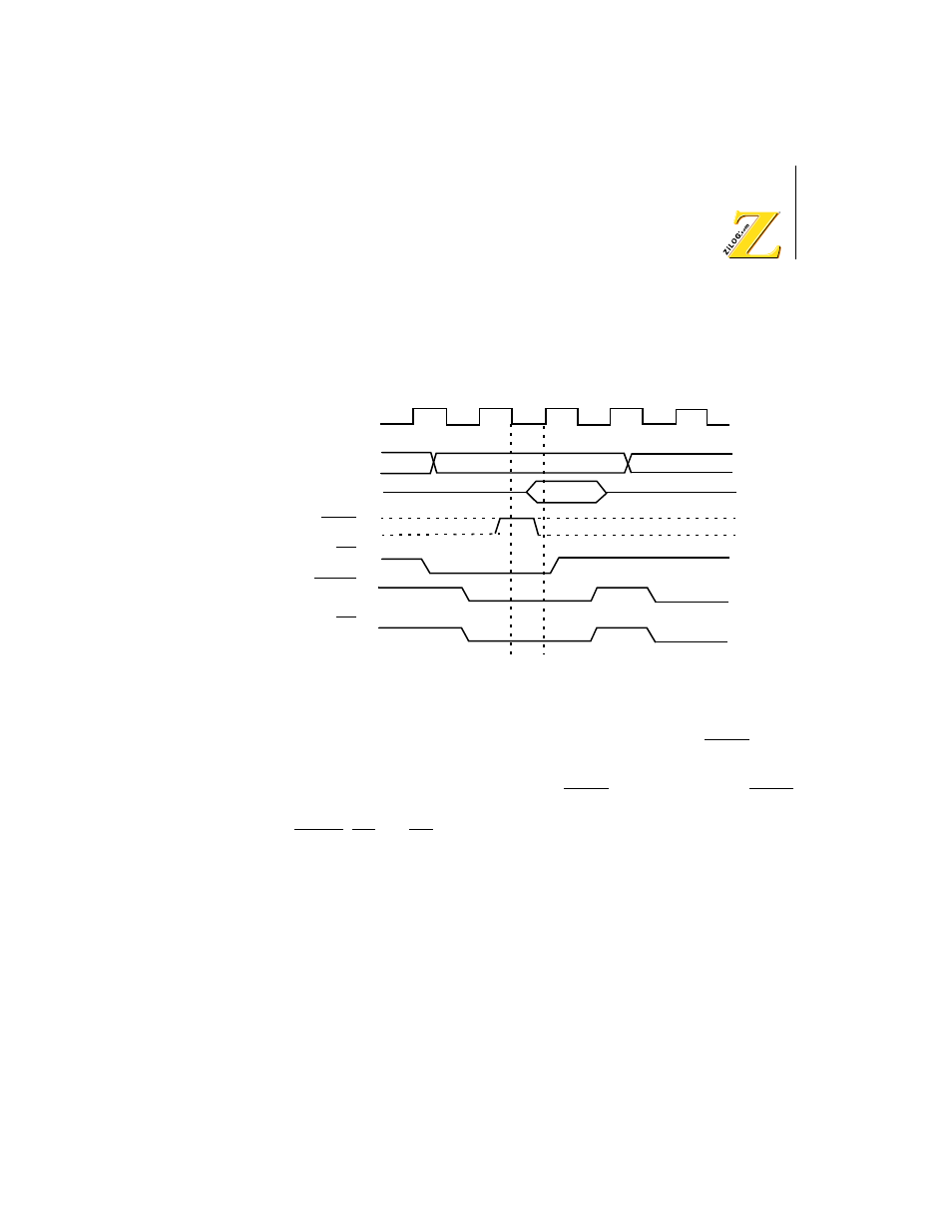
The Op Code on the data bus is latched at the rising edge of T3 and the
bus cycle terminates at the end of T3.
Figure 9.
Op Code Fetch (without Wait State) Timing Diagram
Figure 10 illustrates the insertion of Wait States (TW) into the Op Code
fetch cycle. Wait States (TW) are controlled by the external WAIT input
combined with an on-chip programmable Wait State generator.
At the falling edge of T2 the combined WAIT input is sampled. If WAIT
input is asserted Low, a Wait State (TW) is inserted. The address bus,
MREQ, RD and M1 are held stable during Wait States. When WAIT is
sampled inactive High at the falling edge of TW, the bus cycle enters T3
and completes at the end of T3.
T1
T3
T1
T2
T2
Phi
A0
–
A19
D0
–
D7
M1
MREQ
RD
WAIT