Figure 15. reset timing diagram – Zilog Z80180 User Manual
Page 40
Z8018x
Family MPU User Manual
UM005003-0703
25
The external bus is IDLE while the CPU computes the effective address.
Finally, the computed memory location is written with the contents of the
CPU register (g).
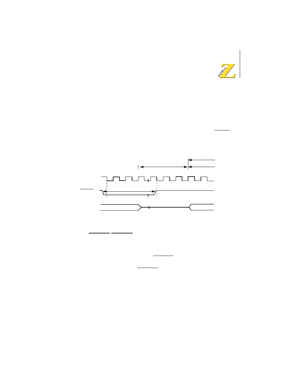
RESET Timing
Figure 15 depicts the Z8X180 hardware RESET timing. If the RESET pin
is Low for six or more clock cycles, processing is terminated and the
Z8X180 restarts execution from (logical and physical) address
00000H
.
Figure 15. RESET Timing Diagram
BUSREQ/BUSACK Bus Exchange Timing
The Z8X180 can coordinate the exchange of control, address and data bus
ownership with another bus master. The alternate bus master can request
the bus release by asserting the BUSREQ (Bus Request) input Low. After
the Z8X180 releases the bus, it relinquishes control to the alternate bus
master by asserting the BUSACK (Bus Acknowledge) output Low.
The bus may be released by the Z8X180 at the end of each machine cycle.
In this context, a machine cycle consists of a minimum of three clock
cycles (more if wait states are inserted) for Op Code fetch, memory read/
write, and I/O read/write cycles. Except for these cases, a machine cycle
corresponds to one clock cycle.
Phi
A0
–
A19
RESET
RESET
High impedance
Restart address (00000H)
RESET Start
Op Code Fetch Cycle
T1
T2
6 or more clocks