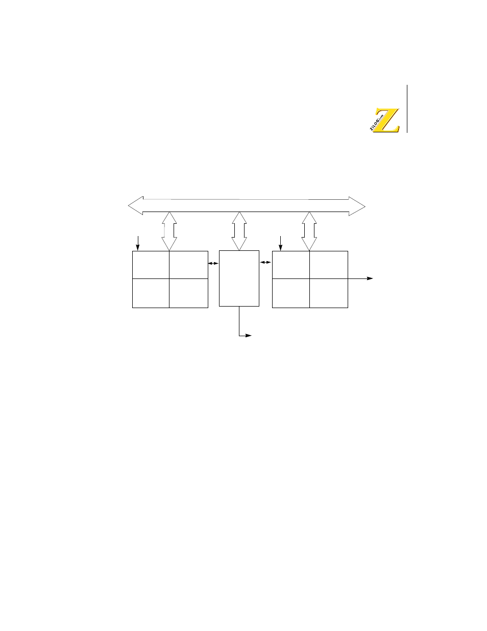
Figure 63. prt block diagram, Prt register description, Z8018x family mpu user manual – Zilog Z80180 User Manual
Page 172
Z8018x
Family MPU User Manual
UM005003-0703
157
control register. The PRT input clock for both channels is equal to the
system clock divided by 20.
Figure 63. PRT Block Diagram
PRT Register Description
Timer Data Register (TMDR: I/O Address - CH0: 0CH, 0DH; CH1: 15H,
14H). PRT0 and PRT1 each contain 16-bit timer Data Registers (TMDR).
TMDR0 and TMDR1 are each accessed as low and high byte registers
(TMDR0H, TMDR0L and TMDR1H, TMDR1L). During RESET,
TMDR0 and TMDR1 are set to
FFFFH
.
TMDR is decremented once every twenty clocks. When TMDR counts
down to 0, it is automatically reloaded with the value contained in the
Reload Register (RLDR).
TMDR is read and written by software using the following procedures.
The read procedure uses a PRT internal temporary storage register to
Phi
¸ 20
Internal Address/Data Bus
TOUT
Timer Data
Register 0L
: TMDR0L (8)
Timer Data
Register 0H
: TMDR0H (8)
Timer Reload
Register 0L
: RLDR0L (8)
Timer Reload
Register 0H
: RLDR0H (8)
Timer Control
Register
: TCR (8)
Phi
¸ 20
Timer Data
Register 1L
: TMDR1L (8)
Timer Data
Register 1H
: TMDR1H (8)
Timer Reload
Register 1L
: RLDR1L (8)
Timer Reload
Register 1H
: RLDR1H (8)
Interrupt Register