Figure 13. i/o read/write timing diagram – Zilog Z80180 User Manual
Page 38
Z8018x
Family MPU User Manual
UM005003-0703
23
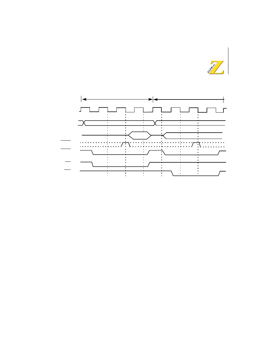
Figure 13. I/O Read/Write Timing Diagram
Basic Instruction Timing
An instruction may consist of a number of machine cycles including Op
Code fetch, operand fetch, and data read/write cycles. An instruction may
also include cycles for internal processes which make the bus IDLE. The
example in Figure 14 illustrates the bus timing for the data transfer
instruction LD (IX+d),g.
T1
T1
T2
TW
T3
T2
T3
Phi
A0
–
A19
D0
–
D7
WR
IORQ
RD
WAIT
I/O Read Cycle
I/O Write Cycle
Write data
TW
I/O address
I/O address
Read data