Control and status register address maps, Visual example, Reads the first data buffer, in 16-byte bursts – Digi NS9215 User Manual
Page 368
I / O H U B M O D U L E
Control and status register address maps
368
Hardware Reference NS9215
31 March 2008
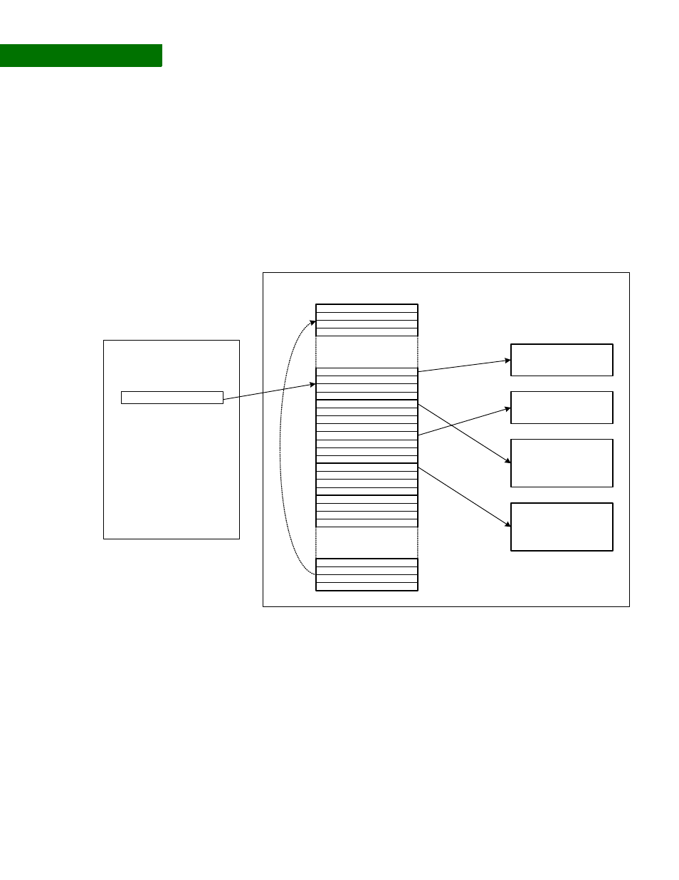
2
Verifies that the data buffer is valid by making sure the F bit is set to 1.
3
Reads the first data buffer, in 16-byte bursts.
4
Continues to process the buffer descriptors and data buffers until all data has
been transmitted from the buffer descriptor with the L bit set to 1. The DMA
controller interrupts the CPU if the I bit is set to a 1.
5
Remains in the IDLE state until the channel enable bit is set to a 0, then set to a
1 again.
Visual example
. . . . . . . . . . . . . . . . . . . . . . . . . . . . . . . . . . . . . . . . . . . . . . . . . . . . . . . . . . . . . . . . . . . . . . . . . . . . . . . . . .
C o n t r o l a n d s t a t u s r e g i s t e r a d d r e s s m a p s
The I/O Hub provides a series of registers for the low speed peripheral modules it
supports. The DMA, direct mode, and interrupt control register formats are the
same for these modules. The base address for the registers is 0x9000_0000. Write
buffering in the MMU must be disabled for all registers in the I/O Hub address space,
from address 0x9000_0000 to 0x9FFF_FFFF.
Register address maps are shown for each low speed peripheral module.
Buffer Pointer = null
Buffer Length = null
W=0 , I=0 , L=0 , F=0
Buffer Pointer = 0x 200
Buffer Length = 0x 012
W=0 , I=0 , L=0 , F=1
Buffer Pointer = 0x 400
Buffer Length = 0x 064
W=0 , I=1 , L=1 , F=1
Buffer Pointer = 0x 300
Buffer Length = 0x 018
W=0 , I=0 , L=0 , F=1
Buffer Pointer = 0x 500
Buffer Length = 0x 064
W=0 , I=1 , L=1 , F=1
Buffer Pointer = null
Buffer Length = null
W=0 , I=0 , L=0 , F=0
Buffer Pointer = null
Buffer Length = null
W=1 , I=0 , L=0 , F=0
System Memory
I/O Hub DMA Controller
TXBDP + INDEX
(first buffer in packet)
18 byte data buffer
24 byte data buffer
100 byte data buffer
100 byte data buffer
(last buffer in packet)