Registers register bit assignment – Digi NS9215 User Manual
Page 196
S Y S T E M C O N T R O L M O D U L E
System Memory Chip Select 2 Static Memory Base and Mask registers
196
Hardware Reference NS9215
Registers
Register bit
assignment
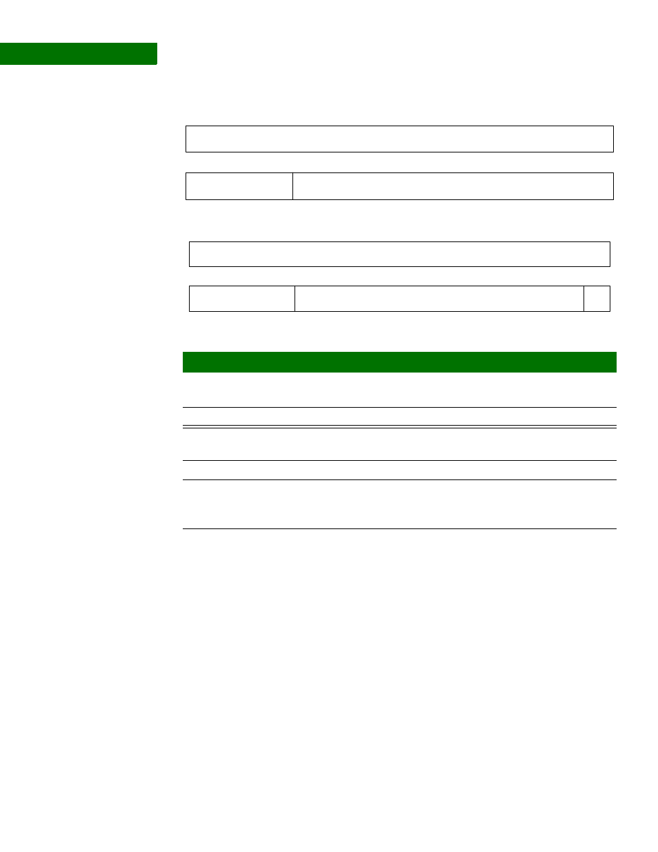
S y s t e m M e m o r y C h i p S e l e c t 2 S t a t i c M e m o r y B a s e a n d M a s k
. . . . . . . . . . . . . . . . . . . . . . . . . . . . . . . . . . . . . . . . . . . . . . . . . . . . . . . . . . . . . . . . . . . . . . . . . . . . . . . . . .
r e g i s t e r s
Addresses: A090 0200 / 0204
These control registers set the base and mask for system memory chip select 2, with
a minimum size of 4K. The powerup default settings produce a memory range of
0x6000 0000 — 0x6FFF FFFF
.
13
12
11
10
9
8
7
6
5
4
3
2
1
0
15
14
31
29
28
27
26
25
24
23
22
21
20
19
18
17
16
30
Chip select 1 base (CS1B)
Reserved
Chip select 1 base (CS1B)
13
12
11
10
9
8
7
6
5
4
3
2
1
0
15
14
31
29
28
27
26
25
24
23
22
21
20
19
18
17
16
30
Chip select 1 mask (CS1M)
Reserved
Chip select 1 mask (CS1M)
CSD1
Bits
Access
Mnemonic
Reset
Description
D31:12
R/W
CS1B
0x50000
Chip select 1 base
Base address for chip select 1
D11:00
N/A
Reserved
N/A
N/A
D31:12
R/W
CS1M
0xF0000
Chip select 1 mask
Mask or size for the chip select 1.
D11:01
N/A
Reserved
N/A
N/A
D00
R/W
CSD1
0x1
Chip select 1 disable
0
Disable chip select
1
Enable chip select