Control register, Reset values – Digi NS9215 User Manual
Page 232
M E M O R Y C O N T R O L L E R
Control register
232
Hardware Reference NS9215
Reset values
Reset values will be noted in the description column of each register table, rather
than as a separate column.
. . . . . . . . . . . . . . . . . . . . . . . . . . . . . . . . . . . . . . . . . . . . . . . . . . . . . . . . . . . . . . . . . . . . . . . . . . . . . . . . . .
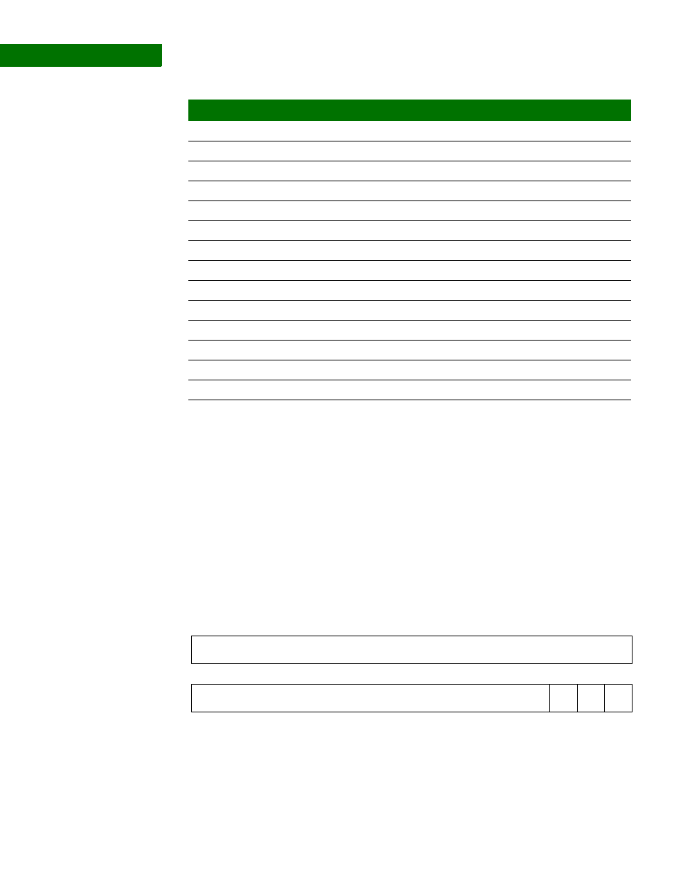
C o n t r o l r e g i s t e r
Address: A070 0000
The Control register controls the memory controller operation. The control bits can
be changed during normal operation.
Register
A070 0240
StaticConfig2
Static Memory Configuration Register 2
A070 0244
StaticWaitWen2
Static Memory Write Enable Delay 2
A070 0248
StaticWaitOen2
Static Memory Output Enable Delay 2
A070 024C
StaticWaitRd2
Static Memory Read Delay 2
A070 0250
StaticWaitPage2
Static Memory Page Mode Read Delay 2
A070 0254
StaticWaitWr2
Static Memory Write Delay 2
A070 0258
StaticWaitTurn2
Static Memory Turn Round Delay 2
A070 0260
StaticConfig3
Static Memory Configuration Register 3
A070 0264
StaticWaitWen3
Static Memory Write Enable Delay 3
A070 0268
StaticWaitOen3
Static Memory Output Enable Delay 3
A070 026C
StaticWaitRd3
Static memory Read Delay 3
A070 0270
StaticWaitPage3
Static Memory Page Mode Read Delay 3
A070 0274
StaticWaitWr3
Static Memory Write Delay 3
A070 0278
StaticWaitTurn3
Static Memory Turn Round Delay 3
Address
Register
Description
MCEN
13
12
11
10
9
8
7
6
5
4
3
2
1
0
15
14
31
29
28
27
26
25
24
23
22
21
20
19
18
17
16
30
Reserved
Reserved
LPM ADDM