Peripheral dma write access – Digi NS9215 User Manual
Page 343
. . . . .
E X T E R N A L D M A
Peripheral DMA write access
www.digiembedded.com
343
Peripheral DMA
single read access
Peripheral DMA
burst read access
. . . . . . . . . . . . . . . . . . . . . . . . . . . . . . . . . . . . . . . . . . . . . . . . . . . . . . . . . . . . . . . . . . . . . . . . . . . . . . . . . .
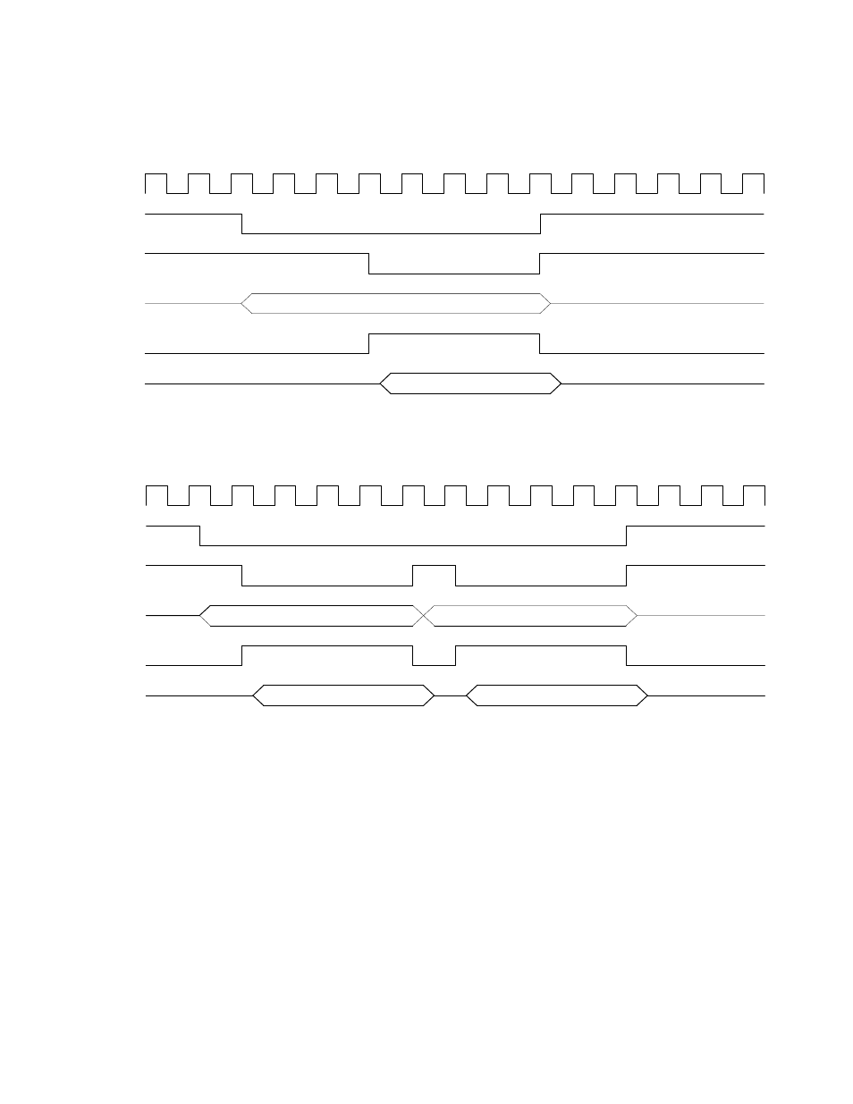
P e r i p h e r a l D M A w r i t e a c c e s s
The diagrams in this section describe how the DMA engine performs write accesses
of an external peripheral. The CLK signal shown is for reference, and its frequency
is equal to the speed grade of the part. For peripheral writes, the PDEN signal is an
AND function of the active status of
st_cs_n[n]
and
we_n
. Write data into the
peripheral on the falling edge of the PDEN signal. Data and control signals are
always held after the falling edge of PDEN for one reference CLK cycle.
DATA VALID
PDEN
DQ
st_cs_n[n]
CLK
ADDR
Address Valid
st_oe_n
PDEN
DQ
st_cs_n[n]
CLK
DATA0
DATA1
ADDR0
ADDR1
ADDR
st_oe_n