System port pins, Transmit system port pins, Receive system port pins – Rainbow Electronics DS3170 User Manual
Page 76: Table 9-20. tsofi input pin functions, Table 9-21. tsofo/tden/output pin functions, Table 9-22 tclko/tgclk output pin functions, Table 9-20, Table 9-22, Table 9-21
DS3170 DS3/E3 Single-Chip Transceiver
76 of 233
long. The generated BERT signal replaces the data on the TSER pin in framed modes when the BERT is enabled
by setting the PORT.CR1.BENA.
When the BERT is enabled The TDEN and RDEN pins will still be active but the data on the TSER pin will be
discarded.
9.5.8 System Port Pins
The system port pins have multiple functions based on the framing mode the device is in as well as other pin mode
select bits.
9.5.8.1 Transmit System Port Pins
The transmit system pins are TSOFI, TSER, TSOFO / TDEN, and TCLKO / TGCLK. They have different functions
based on the framing mode and other pin mode bits. Unused input pin functions should drive a logic zero into the
device circuits expecting a signal from that pin. The control bits that configure the pins’ modes are
FM[2:0],
TPFPE,
TSOFOS and
TCLKS.
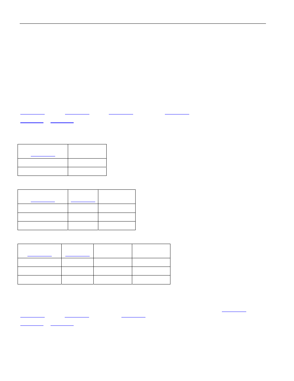
describe the function selected by the FM bits and other pin mode bits for the multiplexed
pins.
Table 9-20. TSOFI Input Pin Functions
FM[2:0]
PIN
FUNCTION
0XX (FRM)
TSOFI
1XX (UFRM)
Not used
Table 9-21. TSOFO/TDEN/Output Pin Functions
FM[2:0]
TSOFOS
PIN
FUNCTION
0XX (FRM)
0
TDEN
0XX (FRM)
1
TSOFO
1XX (UFRM)
X
High
Table 9-22 TCLKO/TGCLK Output Pin Functions
FM[2:0]
TCLKS
PIN
FUNCTION
GAP SOURCE
0XX (FRM)
0
TGCLK
TDEN
0XX (FRM)
1
TCLKO
none
1XX (UFRM)
X
TCLKO
none
9.5.8.2 Receive System Port Pins
The receive system pins are RSER, RSOFO / RDEN and RCLKO / RGCLK. They have different functions based
on the framing mode and other pin mode bits. Unused input pin functions should drive a logic zero into the device
circuits expecting a signal from that pin. The control bits that configure these pins are
FM[2:0],
RPFPE,
RCLKS.
describe the function selected by the FM bits and other pin mode bits for the multiplexed
pins.