Pin descriptions, Short pin descriptions, Hort – Rainbow Electronics DS3170 User Manual
Page 25: Escriptions, Table 7-1. ds3170 short pin descriptions, 7 pin descriptions
DS3170 DS3/E3 Single-Chip Transceiver
25 of 233
7 PIN DESCRIPTIONS
Note: In JTAG mode, all digital pins are bidirectional to increase the effectiveness of board level ATPG patterns for
isolation of interconnect failures.
7.1 Short Pin Descriptions
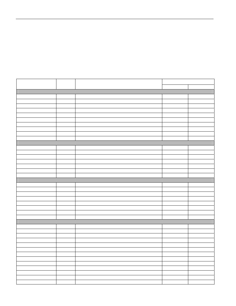
Table 7-1. DS3170 Short Pin Descriptions
Ipu (input with pullup), Oz (output tri-stateable), Oa (Analog output), Ia (analog input), IO (Bidirectional in/out)
PIN
NAME TYPE
FUNCTION
BGA LQFP
Line IO
TLCLK
O
Transmit Line Clock Output
B7 85
TPOS / TDAT
O
Transmit Positive AMI / Data
E9
67
TNEG
O
Transmit Negative AMI
D9
70
TXP
Oa
Transmit Positive analog
E1, E2
12, 13
TXN
Oa
Transmit Negative analog
F1, F2
16, 17
RLCLK
I
Receive Clock Input
A8
81
RXP
Ia
Receive Positive analog
A4
94
RXN Ia
Receive
Negative
analog
A3
97
RPOS / RDAT
Ia
Positive AMI / Data
F10
62
RNEG / RLCV
Ia
Negative AMI / Line Code Violation
F9
63
DS3/E3 Overhead Interface
TOH I
Transmit
Overhead
C7
83
TOHEN I
Transmit
Overhead
Enable
E10
66
TOHCLK O
Transmit
Overhead
Clock
D7
82
TOHSOF
O
Transmit Overhead Start Of Frame
G9
60
ROH O
Receive
Overhead
B6
88
ROHCLK O
Receive
Overhead
Clock
C9
73
ROHSOF
O
Receive Overhead Start Of Frame
F8
61
DS3/E3 Serial Data DS3/E3 Overhead Interface
TCLKI
I
Transmit Line Clock Input
C10
72
TSOFI
I
Transmit Start Of Frame Input
A9
78
TSER
I
Transmit Serial Data
B10
75
TCLKO / TGCLK
O
Transmit Clock Output / Gapped Clock
B9
77
TSOFO / TDEN
O
Transmit Framer Start Of Frame / Data Enable
C8
79
RSER
O
Receive Serial Data
C6
86
RCLKO / RGCLK
O
Receive / Clock Output / Gapped Clock
A6
87
RSOFO / RDEN
O
Receive Framer Start Of Frame / Data Enable
B8
80
Microprocessor Interface
D[15] IO
Data
[15]
G8
58
D[14] IO
Data
[14]
H10
56
D[13] IO
Data
[13]
H9
55
D[12] IO
Data
[12]
H8
54
D[11] IO
Data
[11]
J10
53
D[10] IO
Data
[10]
J9
52
D[9] IO
Data
[9]
G6
40
D[8] IO
Data
[8]
J8
48
D[7]/SPI_CPOL
IO
Data [7] / SPI Interface Clock Polarity
K8
47
D[6]/SPI_CPHA
IO
Data [6] / SPI Interface Clock Phase
H7
46
D[5]/SPI_SWAP
IO
Data [5:3] / SPI Bit Order Swap
J7
45
D[4]
IO
Data [4]
K7
44
D[3] IO
Data
[3]
H6
43