Gl.cr2 – Rainbow Electronics DS3170 User Manual
Page 128
DS3170 DS3/E3 Single-Chip Transceiver
128 of 233
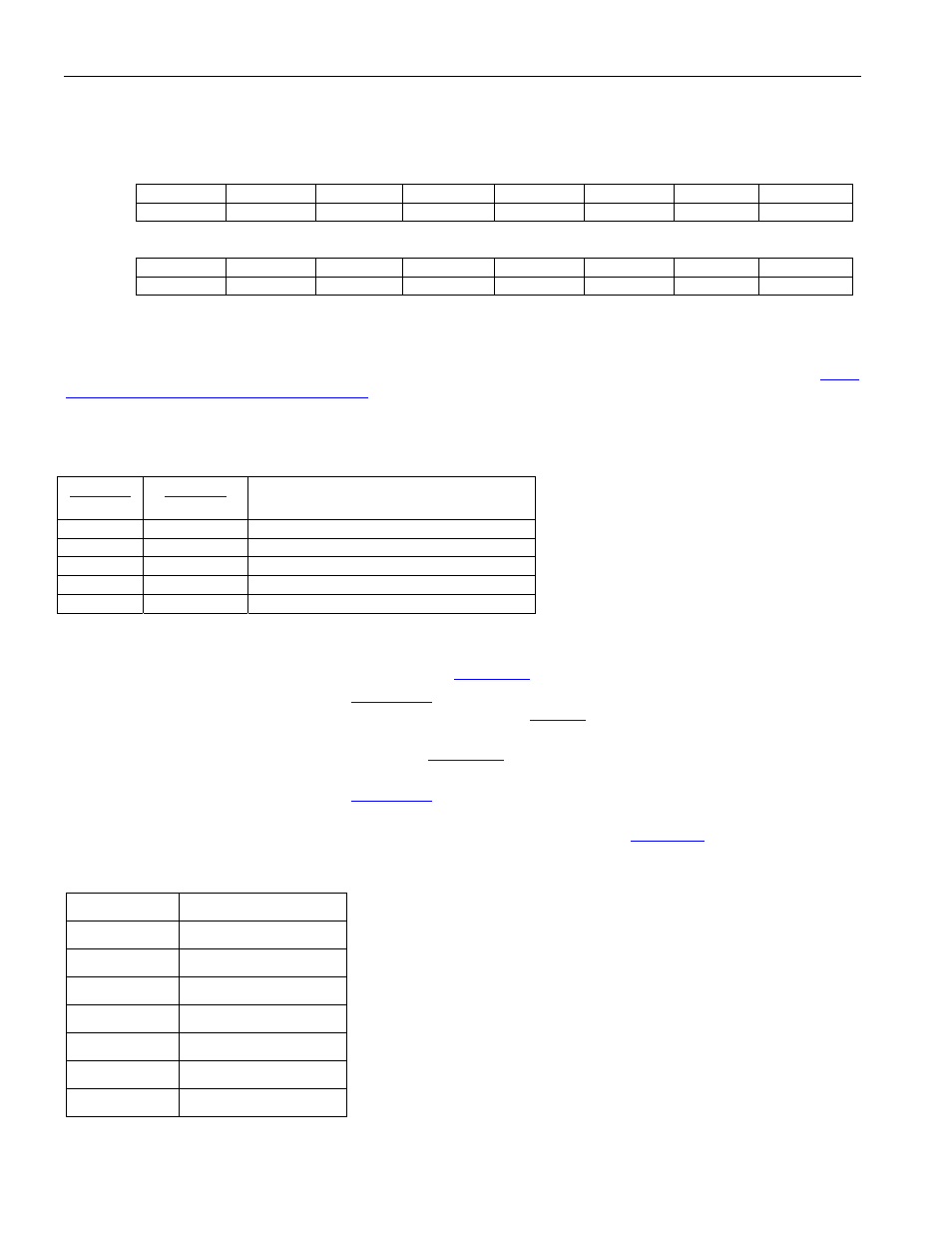
Register Name:
GL.CR2
Register Description:
Global Control Register 2
Register Address:
004h
Bit
# 15 14 13 12 11 10 9 8
Name
-- -- -- --
G8KRS1
G8KRS0
G8K0S
G8KIS
Default
0 0 0 0 0 0 0 0
Bit
# 7 6 5 4 3 2 1 0
Name
-- -- -- --
CLAD2
CLAD1
CLAD0
--
Default
0 0 0 0 0 0 0 0
Bits 11 to 10: Global 8KHz Reference Source [1:0] (G8KRS[1:0]). These bits determine the source for the
internally generated 8 kHz reference as well as the internal one second reference, which is derived from the Global
8 kHz reference. The source is selected from the CLAD clock or from the port 8KREF clock source. See
9-12. Global 8 kHz Reference Source Table
These bits are ignored when the G8KIS bit = 1.
Table 9-12. Global 8 kHz Reference Source Table
G8KIS
G8KRS[1:0]
SOURCE
None, the 8KHZ divider is disabled.
Derived from CLAD output clock
8KREF source selected by P8KRS[1:0]
1 XX
GPIO4
Bit 9: Global 8KHz Reference Output Select (G8KOS). This bit determines whether GPIO2 pin is used for the
global 8KREFO output signal, or is used as specified by
.GPIO2S[1:0].
0 = GPIO2 pin mode selected by
GPIO2S[1:0]
1 = GPIO2 is the global 8KREFO output signal selected by
.8KRS[2:0]
Bit 8: Global 8KHz Reference Input Select (G8KIS). This bit determines whether GPIO4 pin is used for the global
8KREFI input signal, or is used as specified by
.GPIO4S[1:0]. G8KREFI signal will be low if not
selected. Global 8KREF pin signal will be low if not selected.
0 = GPIO4 pin mode selected by
GPIO4S[1:0]
1 = GPIO4 is the global 8KREFI input signal for one second timer and port to use
Bits 3 to 1: CLAD IO Mode [2:0] (CLAD[2:0]). These bits control the CLAD. See
Table 9-11. CLAD Clock Source Settings
CLAD[2:0] REFCLK
(INPUT)
000 44.736
001 34.368
MHz
MHz
100
77.76 MHz
101 Undefined
11X Undefined