Receive line interface pin timing source selection, Receiver framer pin timing source selection – Rainbow Electronics DS3170 User Manual
Page 61
DS3170 DS3/E3 Single-Chip Transceiver
61 of 233
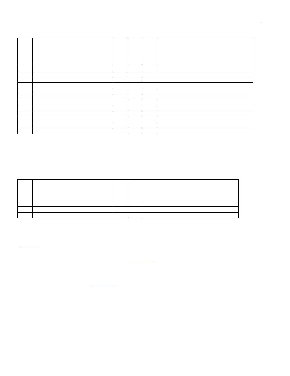
Table 9-7. Transmit Framer Pin Signal Timing Source Select
LOOP
T
LBM[2:0]
LIUEN
CLADC
TFTS
VALID TIMING TO THESE CLOCK PINS
1
XXX
X
X
0
TCLKO, TLCLK, RCLKO
1 XXX 0
X
1
RLCLK
1
XXX
1
X
1
No valid timing to any input clock pin
0
PLB (011) or DLB (100) or ALB 001)
0
X
0
TCLKO, TLCLK, RCLKO
0
PLB (011) or DLB (100)
1
X
0
TCLKO, TLCLK, RCLKO
0
DLB & LLB (110)
X
X
0
TCLKO, RCLKO
0 LLB
(010) X
X
0
TCLKO
0
not LLB, DLB or PLB (00X)
X
X
0
TCLKO, TLCLK
0
not PLB (011)
X
0
1
No valid timing to any input clock pin
0 not
PLB
(011) X
1
1
TCLKI
0 PLB
(011) 0
X
1
RLCLK
0
PLB (011)
1
X
1
No valid timing to any input clock pin
9.2.3.3 Receive Line Interface Pin Timing Source Selection
(RPOS/RDAT, RNEG/RLCV)
The receive line interface signal pin group must clocked in with the RLCLK clock input pin. When the LIU is
enabled, the receive line interface pins are not used so there is no valid clock reference.
Table 9-8. Receive Line Interface Pin Signal Timing Source Select
LOOP
T
LBM[2:0]
LIUEN
CLADC
VALID TIMING TO THESE CLOCK PINS
X XXX 0
X
RLCLK
X
XXX
1
X
No valid timing to any clock pin
9.2.3.4 Receiver Framer Pin Timing Source Selection
(RSER, RSOFO/RDEN)
The receive framer signal pin group has the same functional timing clock source as the RCLKO pin described in
Other clock pins can be used for the external timing. The RCLKO receive clock output pin is always a valid output
clock for external logic to use for these signals when
.RFTS=0.
The receive framer timing select bit (RFTS) is used to select input or output clock pin timing. When RFTS=0, output
clock timing is selected. When RFTS=1, input clock timing is selected. If RFTS is set for input clock timing and an
output clock pin is used, or If RFTS is set for output clock timing and an input clock pin is used, then the setup, hold
and delay timings, as specified in
, will not be valid. There are some combinations of RFTS=1 and other
modes in which there is no input clock pin available for external timing since the clock source is derived internally
from the RX LIU or the CLAD.