Uni mode transmit pin functional timing, Uni mode receive pin functional timing, Figure 7-4 – Rainbow Electronics DS3170 User Manual
Page 39
DS3170 DS3/E3 Single-Chip Transceiver
39 of 233
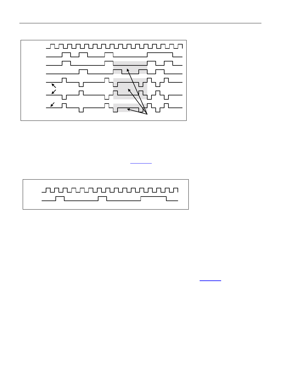
Figure 7-4. Rx Line IO HDB3 Functional Timing Diagram
RLCLK
RPOS
RNEG
(RX DATA)
HDB3 CODEWORD
(RX LINE)
+
-
RXP
RXN
V
V
B
B
B
V
B
V
0 V
BIAS V
7.3.1.3 UNI Mode Transmit Pin Functional Timing
The TDAT pin is available when the line interface is in the UNI mode and the transmit line pins are enabled
The TDAT signal changes a small delay after the positive edge of the reference clock signal if the clock pin is not
inverted, other wise they change after the negative edge. The TLCLK clock pin is the clock reference typically
used for the TDAT signal, but the TDAT can be time referenced to the TCLKI, TCLKO, RLCLK or RCLKO clock
pins. The TDAT pin can be inverted. Please refer to
Figure 7-5. Tx Line IO UNI Functional Timing Diagram
7.3.1.4 UNI Mode Receive Pin Functional Timing
The RDAT pin is available when the line interface is in the UNI mode. The RLCV pin is available when the line
interface is in the UNI Mode.
All bits on the RDAT pin, will come out the RSER pin, if the RSER pin is enabled.
The signal on the RLCV pin enables the BPV counter, which is in the line interface, to increment each clock it is
high.
The RDAT and RLCV signals are sampled at the rising edge of the reference clock signal if the clock pin is not
inverted, otherwise they are sampled at the negative edge. The RLCLK clock pin is the clock reference used for the
RDAT and RLCV signals. The RDAT and RLCV pins can be inverted. Please refer to
TLCLK
TDAT