Gapped clocks, Reset and power-down, Eset and – Rainbow Electronics DS3170 User Manual
Page 63: Ower, Figure 9-4. example io pin clock muxing, 3 reset and power-down, 5 gapped clocks
DS3170 DS3/E3 Single-Chip Transceiver
63 of 233
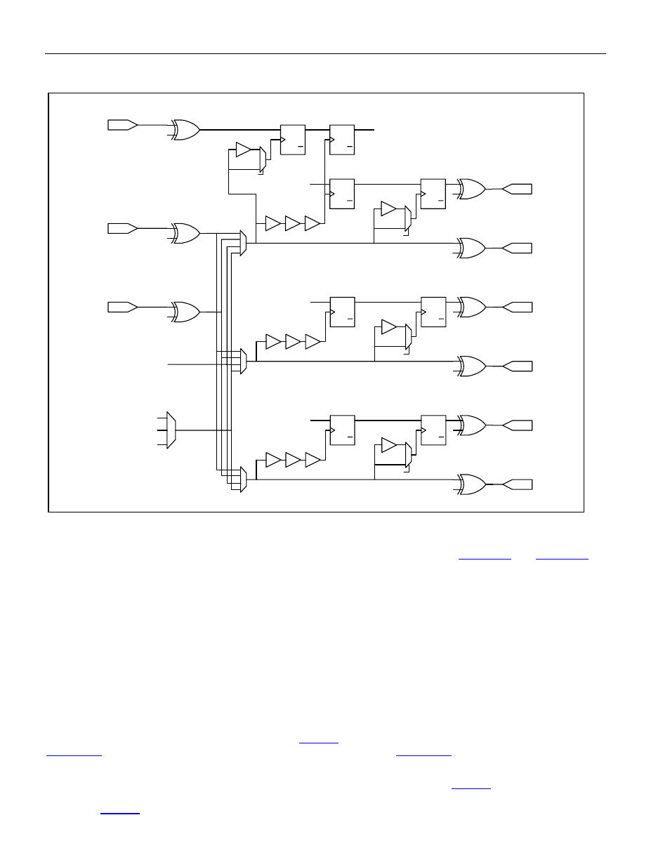
Figure 9-4. Example IO Pin Clock Muxing
Q
Q
SET
CLR
D
INTERNAL
SIGNAL
TCLKI
PIN INVERT
RLCLK
PIN INVERT
RX LIU CLK
DS3 CLK
E3 CLK
STS-1 CLK
CLAD CLOCKS
TCLKO
PIN INVERT
CLOCK TREE
TDEN
PIN INVERT
Q
Q
SET
CLR
D
DELAY
TFTS
0
1
TSER
PIN INVERT
Q
Q
SET
CLR
D
Q
Q
SET
CLR
D
INTERNAL
SIGNAL
DELAY
0
1
TFTS
Q
Q
SET
CLR
D
INTERNAL
SIGNAL
TLCLK
PIN INVERT
CLOCK TREE
TPOS
PIN INVERT
Q
Q
SET
CLR
D
DELAY
TLTS
0
1
Q
Q
SET
CLR
D
INTERNAL
SIGNAL
RCLKO
PIN INVERT
CLOCK TREE
RSER
PIN INVERT
Q
Q
SET
CLR
D
DELAY
RFTS
0
1
9.2.5 Gapped
Clocks
The transmit and receive output clocks can be gapped in certain configurations. See
for
the configuration settings. The gapped clocks are active during DS3 or E3 framed payload bits overhead bits
depending on which mode the device is configured for.
In the internal DS3 or E3 frame modes, the transmit gapped clock is created by the logical OR of the TCLKO and
TDEN signals creating a positive or negative clock edge for each payload bit, the receive gapped clock is created
by the logical OR of the RCLKO and RDEN signals.
When the output clock is disabled, the gapped output signal is high during clock periods if the pin is not inverted,
otherwise it will be low.
The gapped clocks are very useful when the data being clocked does not need to be aligned with any frame
structure. The data is simply clocked one bit at a time as a continuous data stream.
9.3 Reset
and
Power-Down
The device can be reset at a global level via the
RST bit or the
RST pin and at the port level via the
RST bit and the port can be explicitly powered down via the
PD bit. The JTAG logic is reset
using the power on reset signal from one of the LIUs as well as from the
JTRST pin.
The external
RST pin and the global reset bit in the global configuration register (
.RST) are combined to
create an internal global reset signal. The global reset signal resets all the status and control registers on the chip,
except the
RST bit, to their default values and resets all the other flops in the global logic and port to their