B3zs/hdb3/ami mode receive pin functional timing, Figure 7-2 – Rainbow Electronics DS3170 User Manual
Page 38
DS3170 DS3/E3 Single-Chip Transceiver
38 of 233
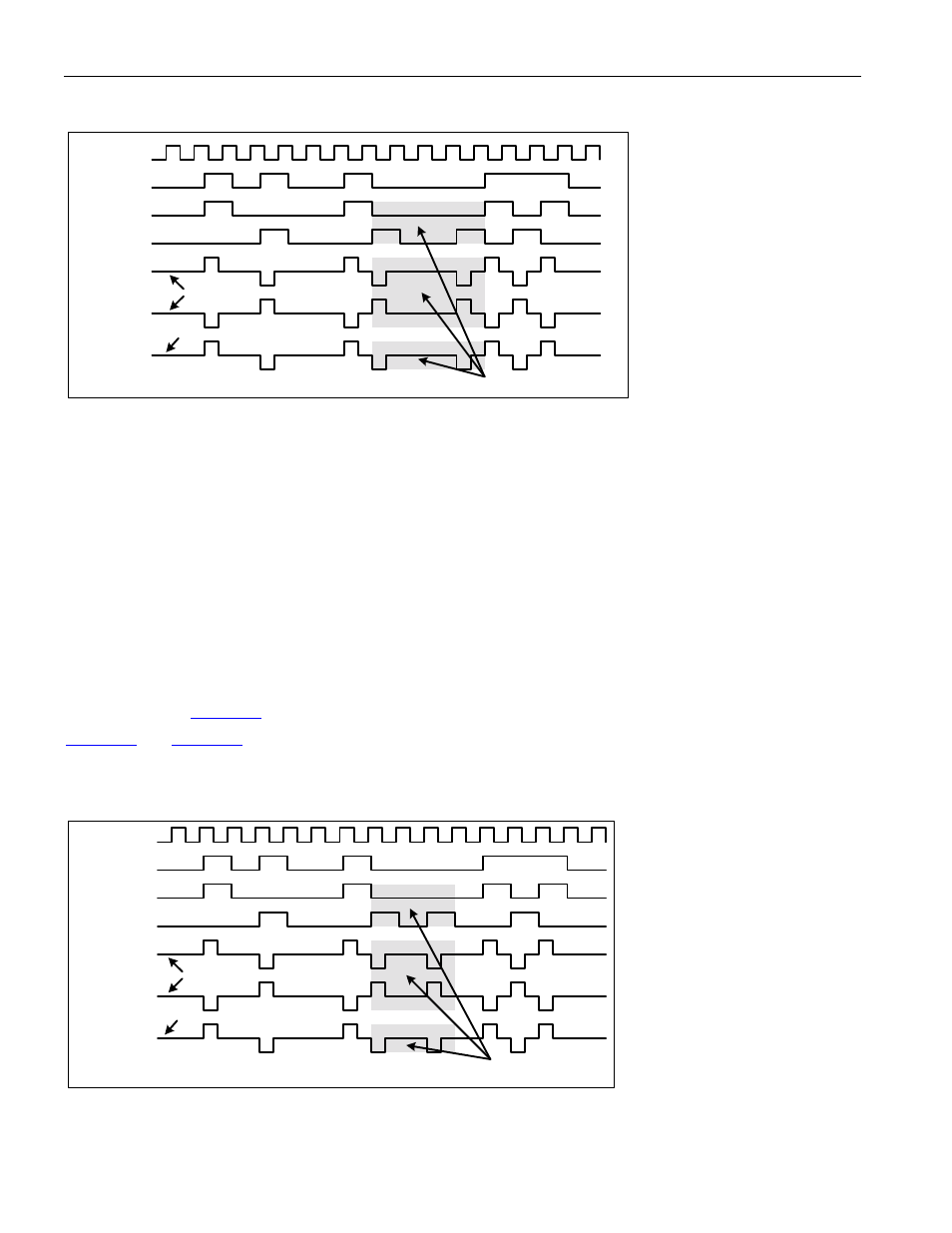
Figure 7-2. Tx Line IO HDB3 Functional Timing Diagram
TLCLK
TPOS
TNEG
(TX DATA)
HDB3 CODEWORD
(TX LINE)
+
-
TXP
TXN
V
V
B
B
B
V
B
V
0 V
BIAS V
7.3.1.2 B3ZS/HDB3/AMI Mode Receive Pin Functional Timing
There is no suggested time alignment between the RXP, RXN and RX LINE signals and the RLCLK clock signal.
The RX DATA signal is not an always readily available signal, it is meant to represent the data value of the other
signals. The signal on RSER in framed mode will be the same as the RX DATA signal except delayed.
The RXP and RXN pins are only available when the line is in B3ZS/HDB3 or AMI mode and the LIU is enabled.
The RPOS, RNEG and RLCLK pins are only available when the line is in B3ZS/HDB3 or AMI mode and the LIU is
disabled.
The RPOS and RNEG signals are sampled at the rising edge of the reference clock signal if the clock pin is not
inverted, otherwise they are sampled at the negative edge. The RLCLK clock pin is the clock reference used for the
RPOS and RNEG signals. The RPOS and RNEG pins can be inverted.
RXP and RXN are differential analog input pins. They are biased around ½ VDD and pulse above and below the
bias voltage by about 1 Volt with zero cable length. These signals are connected to the windings of a 1:2 step up
transformer and the other winding of the transformer is connected to the RX LINE signal. The RX LINE signal is a
bipolar signal that pulses about 1 Volt positive and 1 Volt negative above and below ground (0 volts) with zero
cable length. See
for a diagram of the external connections.
show the relationship between the analog and the digital outputs.
Figure 7-3. Rx Line IO B3ZS Functional Timing Diagram
RLCLK
RPOS
RNEG
(RX DATA)
B3ZS CODEWORD
(RX LINE)
+
-
RXP
RXN
V
V
B
B
B
V
B
V
0 V
BIAS V