Rainbow Electronics DS2143Q User Manual
Features, Description, Pin assignment
E
Copyright 1997 by Dallas Semiconductor Corporation.
All Rights Reserved. For important information regarding
patents and other intellectual property rights, please refer to
Dallas Semiconductor data books.
DS2143/DS2143Q
E1 Controller
DS2143/DS2143Q
031397 1/40
FEATURES
•
E1/ISDN–PRI framing transceiver
•
Frames to CAS, CCS, and CRC4 formats
•
Parallel Control Port
•
Onboard two frame elastic store slip buffer
•
Extracts and inserts CAS signaling bits
•
Programmable output clocks for fractional E1 links,
DS0 loopbacks, and Drop and Insert applications
•
Onboard Sa data link support circuitry
•
FEBE E–Bit Detection, Counting and Generation
•
Pin compatible with DS2141A T1 Controller
•
5V supply; low power (50 mW) CMOS
•
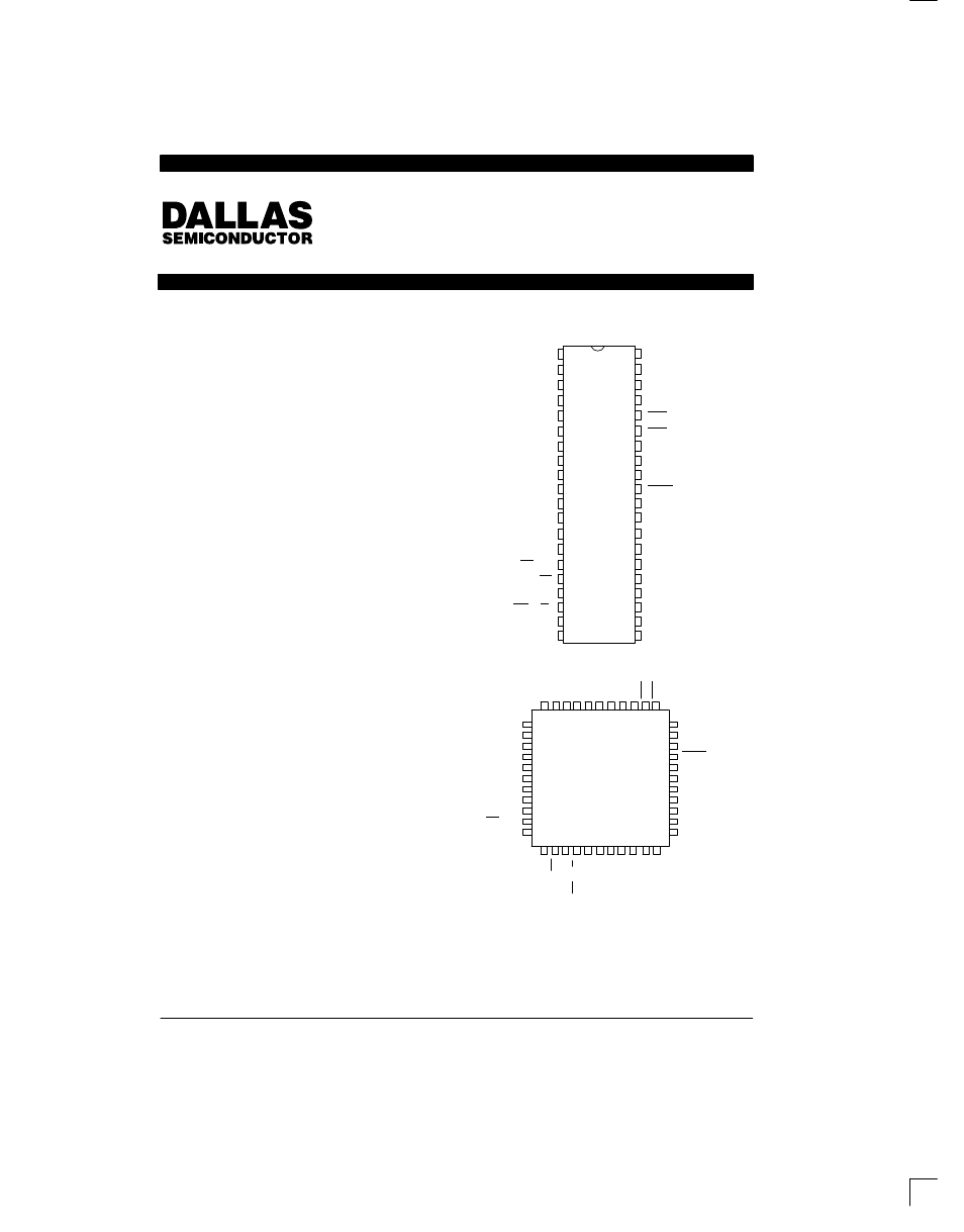
Available in 40–pin DIP and 44–pin PLCC (DS2143Q)
DESCRIPTION
The DS2143 is a comprehensive, software–driven E1
framer. It is meant to act as a slave or coprocessor to a
microcontroller or microprocessor. Quick access via
the parallel control port allows a single micro to handle
many E1 lines. The DS2143 is very flexible and can be
configured into numerous orientations via software.
The software orientation of the device allows the user to
modify their design to conform to future E1 specification
changes. The controller contains a set of 69 eight–bit
internal registers which the user can access. These
internal registers are used to configure the device and
obtain information from the E1 link. The device fully
meets al l of the latest E1 specifications including CCITT
G.704, G.706, and G.732.
PIN ASSIGNMENT
LI_SDI
LI_CS
RD (DS)
1
2
3
4
5
6
7
8
9
10
11
12
13
14
15
16
17
18
19
20
21
22
23
24
40–PIN DIP (600 MIL)
25
26
27
28
29
30
31
32
33
34
35
36
37
38
39
40
TCLK
TSER
TCHCLK
TPOS
TNEG
AD0
AD1
AD2
AD3
AD4
AD5
AD6
AD7
BTS
RD(DS)
CS
ALE(AS)
WR(R/W)
RLINK
VSS
VDD
TSYNC
TLINK
TLCLK
INT1
INT2
RLOS/LOTC
TCHBLK
RCHBLK
LI_CS
LI_CLK
SYSCLK
RNEG
RPOS
RSYNC
RSER
RCHCLK
RCLK
RLCLK
LI_SDI
1
2
3
4
5
6
44 43 42 41 40
1819 202122 2324 25 26 27 28
TNEG
TPOS
TCHCLK
TSER
TCLK
VDD
TSYNC
TLINK
TLCLK
INT1
INT2
NC
CS
ALE(AS)
WR(R/W)
RLINK
VSS
RLCLK
RCLK
RCHCLK
RSER
RSYNC
44–PIN PLCC
AD0
AD1
AD2
AD3
AD4
AD5
AD6
AD7
BTS
NC
RLOS/LOTC
TCHBLK
RCHBLK
LI_CLK
NC
NC
SYSCLK
RNEG
RPOS
7
8
9
10
11
12
13
14
15
16
17
39
38
37
36
35
34
33
32
31
30
29