Rainbow Electronics DS1875 User Manual
Ds1875, Pon triplexer and sfp controller, General description
General Description
The DS1875 controls and monitors all functions for burst-
mode transmitters, APD receivers, and video receivers.
It also includes a power-supply controller for APD bias
generation, and provides all SFF-8472 diagnostic and
monitoring functionality. The combined solution of the
DS1875 and the MAX3643 laser driver provides APC
loop, modulation current control, and eye safety func-
tionality. Ten ADC channels monitor V
CC
, temperature
(both internal signals), and eight external monitor inputs
(MON1–MON8) that can be used to meet transmitter,
digital receiver, video receiver, and APD receiver-signal
monitoring requirements. Four total DAC outputs are
available. A PWM controller with feedback and compen-
sation pins can be used to generate the bias for an APD
or as a step-down converter. Five I/O pins allow addi-
tional monitoring and configuration.
Applications
BPON, GPON, or EPON Optical Triplexers
SFF, SFP, and SFP+ Transceiver Modules
APD Controller
Features
♦ Meets All PON Burst-Timing Requirements for
Burst-Mode Operation
♦ Laser Bias Controlled by APC Loop and
Temperature Lookup Table (LUT)
♦ Laser Modulation Controlled by Temperature LUT
♦ Six Total DACs: Four External, Two Internal
♦ Two 8-Bit DACs, One of Which is Optionally
Controlled by MON4 Voltage
♦ Internal 8-Bit DAC Controlled by a Temperature-
Indexed LUT
♦ PWM Controller
♦ Boost or Buck Mode
♦ Boost Mode: Uses Optional External
Components, Up to 90V Bias Generation
♦ 131kHz, 262kHz, 525kHz, or 1050kHz Selectable-
Switching Frequency
♦ APD Overcurrent Protection Using Optional Fast
Shutdown
♦ 10 Analog Monitor Channels: Temperature, V
CC
,
Eight Monitors
♦ Internal, Factory-Calibrated Temperature Sensor
♦ RSSI with 29dB Electrical Dynamic
♦ Five I/O Pins for Additional Control and
Monitoring Functions, Four of Which are Either
Digital I/O or Analog Monitors
♦ Comprehensive Fault-Measurement System with
Maskable Laser Shutdown Capability
♦ Two-Level Password Access to Protect
Calibration Data
♦ 120 Bytes of Password-1 Protected Memory
♦ 128 Bytes of Password-2 Protected Memory in
Main Device Address
♦ 256 Additional Bytes Located at A0h Slave
Address
♦ I
2
C-Compatible Interface for Calibration and
Monitoring
♦ 2.85V to 3.9V Operating Voltage Range
♦ -40°C to +95°C Operating Temperature Range
♦ 38-Pin TQFN (5mm x 7mm) Package
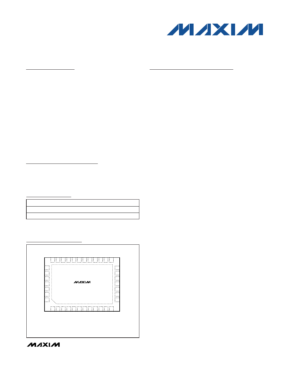
DS1875
________________________________________________________________
Maxim Integrated Products
1
TOP VIEW
TQFN
(5mm
×
7mm
×
0.8mm)
13
14
15
16
17
18
19
MON5/D0
MON6/D1
MON7/D2
MON8/D3
MON1
MON2
MON4
38
37
36
35
34
33
32
1
2
3
4
5
6
7
8
9
10
11
12
N.C.
N.C.
N.C.
V
CC
SW
GND
GND
LOSI
N.C.
GND
V
CC
TX-D
N.C.
FETG
N.C.
TX-F
SCL
SDA
BEN
31
30
29
28
27
26
25
24
23
22
21
20
N.C.
MON3N
MON3P
DAC1
GND
M4DAC
FB
BIAS
MOD
COMP
BMD
V
CC
+
*EP
*EXPOSED PAD.
DS1875
Pin Configuration
Ordering Information
Rev 1; 10/08
For pricing, delivery, and ordering information, please contact Maxim Direct at 1-888-629-4642,
or visit Maxim’s website at www.maxim-ic.com.
+
Denotes a lead-free/RoHS-compliant package.
T&R = Tape and reel.
*
EP = Exposed pad.
PART
TEMP RANGE
PIN-PACKAGE
DS1875T+
-40°C to +95°C
38 TQFN-EP*
DS1875T+T&R
-40°C to +95°C
38 TQFN-EP*
PON Triplexer and SFP Controller
Document Outline
- General Description
- Applications
- Ordering Information
- Pin Configuration
- Features
- Table of Contents
- Absolute Maximum Ratings
- Recommended Operating Condit...
- AC Electrical Characteristics
- Electrical Characteristics (...
- Analog Input Characteristics...
- Analog Output Characteristics
- PWM Characteristics
- Timing Characteristics (Cont...
- Analog Voltage Monitoring
- Digital Thermometer
- Nonvolatile Memory Character...
- I2C Timing Specifications
- Typical Operating Characteri...
- Pin Description
- Block Diagram
- Typical Operating Circuit
- Detailed Description
- BIAS Control
- Modulation Control
- BIAS and MOD Output During P...
- BIAS and MOD Output as a Fun...
- APC and Quick-Trip Shared Co...
- Monitors and Fault Detection
- Transmit Fault (TX-F) Output
- Safety Shutdown (FETG) Output
- Determining Alarm Causes Usi...
- Die Identification
- Low-Voltage Operation
- Enhanced RSSI Monitoring (Du...
- PWM Controller
- DAC1 Output
- M4DAC Output
- Digital I/O Pins
- I2C Communication
- Memory Map
- Register Descriptions
- Lower Memory Register Map
- Table 00h Register Map
- Table 01h Register Map
- Table 02h Register Map
- Table 03h Register Map
- Table 04h Register Map
- Table 05h Register Map
- Table 06h Register Map
- Table 07h Register Map
- Table 08h Register Map
- Auxiliary A0h Memory Registe...
- Lower Memory Register Descri...
- Table 00h Register Descriptions
- Table 01h Register Descriptions
- Table 02h Register Descriptions
- Table 03h Register Descriptions
- Table 04h Register Descriptions
- Table 05h Register Descriptions
- Table 06h Register Descriptions
- Table 07h Register Descriptions
- Table 08h Register Descriptions
- Auxiliary Memory A0h Registe...
- Revision History