Dc electrical characteristics, Table 16-1. recommended dc operating conditions, Table 16-2. dc electrical characteristics – Rainbow Electronics DS3170 User Manual
Page 216: 16 dc electrical characteristics, Absolute maximum ratings
DS3170 DS3/E3 Single-Chip Transceiver
216 of 233
16 DC ELECTRICAL CHARACTERISTICS
ABSOLUTE MAXIMUM RATINGS
Voltage Range on Any Input, Bidirectional or Open Drain
Output Lead with Respect to V
SS
……………………………………………………………………………..-0.3V to +5.5V
Supply Voltage Range (V
DD
) with Respect to V
SS
..…………………………………………………………-0.3V to +3.63V
Ambient Operating Temperature Range……………………………………………………………………..-40°C to +85°C
Junction Operating Temperature Range……………………………………………………………………-40°C to +125°C
Storage Temperature Range………………………………………………………………………………...-55°C to +125°C
Soldering Temperature Range……………………………………………………..See IPC/JEDEC J-STD-020 Standard
These are stress ratings only and functional operation of the device at these or any other conditions beyond those indicated in the operation
sections of this specification is not implied. Exposure to absolute maximum rating conditions for extended periods of time can affect reliability.
Ambient Operating Temperature Range is assuming the device is mounted on a JEDEC standard test board in a convection cooled JEDEC test
enclosure.
Note: The typical values listed below are not production tested.
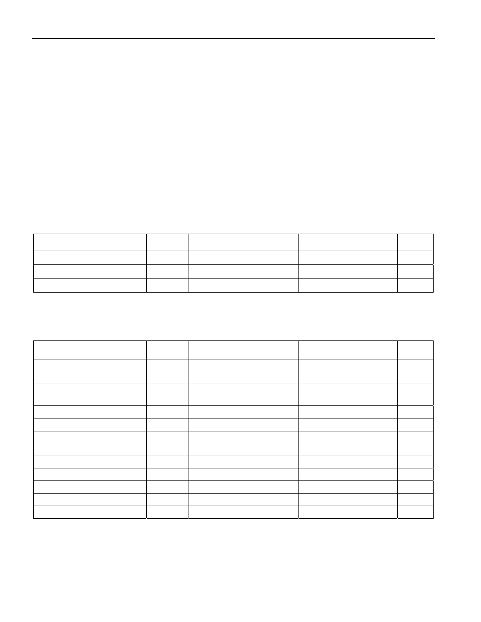
Table 16-1. Recommended DC Operating Conditions
(V
DD
= 3.3V
±5%, T
j
= -40°C to +85°C.)
PARAMETER SYMBOL
CONDITIONS MIN
TYP
MAX
UNITS
Logic 1
V
IH
2.4 5.5 V
Logic 0
V
IL
-0.3 +0.8 V
Supply (V
DD
) ±5%
V
DD
3.135 3.300 3.465 V
Table 16-2. DC Electrical Characteristics
(T
j
= -40°C to +85°C.)
PARAMETER SYMBOL CONDITIONS MIN
TYP
MAX
UNITS
Supply Current
(V
DD
= 3.465V)
I
DD
(Notes
1,
2)
120 145 mA
Power-Down Current
(All DISABLE Bits Set)
I
DDD
(Note
2)
18 25 mA
Lead Capacitance
C
IO
7 pF
Input Leakage
I
IL
-10 +10
mA
Input Leakage (Input Pins
with Internal Pullup Resistors)
I
ILP
-350
+10
mA
Output Leakage (when Hi-Z)
I
LO
-10
+10
mA
Output Voltage (I
OH
= -4.0mA)
V
OH
4mA
outputs,
V
DD
= 3.135
2.4
V
Output Voltage (I
OL
= 4.0mA)
V
OL
4mA
outputs,
V
DD
= 3.135
0.4
V
Output Voltage (I
OH
= -6.0mA)
V
OH
6mA
outputs,
V
DD
= 3.135
2.4
V
Output Voltage (I
OL
= 6.0mA)
V
OL
6mA
outputs,
V
DD
= 3.135
0.4
V
Note 1:
Mode DS3 line rate, all outputs enabled.
Note 2:
All outputs loaded with rated capacitance; all inputs between V
DD
and V
SS
; inputs with pullups connected to V
DD
.