Rainbow Electronics MAX14821 User Manual
General description, Applications, Features
MAX14821
IO-Link Device Transceiver
����������������������������������������������������������������� Maxim Integrated Products 1
19-5916; Rev 0; 8/11
General Description
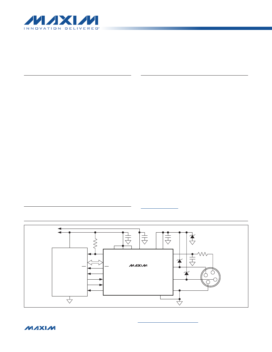
The MAX14821 transceiver is suitable for IO-Link
®
devices and 24V binary sensors/actuators. All specified
IO-Link data rates are supported. In IO-Link applica-
tions, the transceiver acts as the physical layer interface
to a microcontroller running the data-link layer protocol.
Additional 24V digital inputs and outputs are provided.
Two internal linear regulators generate common sensor
and actuator power requirements: 5V and 3.3V.
On-board C/Q and DO drivers are independently config-
urable for push-pull, high-side (PNP), or low-side (NPN)
operation. The device detects the IO-Link C/Q wake-up
condition and generates a wake-up signal on the active-
low WU output. The C/Q and DI inputs have selectable
current loads for use in actuators.
An SPI™ interface allows configuration and monitoring of
the device. Extensive alarm conditions are detected and
communicated through the IRQ output and the SPI inter-
face. The device features reverse-polarity, short-circuit,
and thermal protection. All power lines are monitored for
undervoltage conditions.
The C/Q and DO drivers are specified for sourcing/sink-
ing up to 100mA.
The device is available in a 2.5mm x 2.5mm, 25-pin WLP
and a 4mm x 4mm, 24-pin TQFN package. Both are speci-
fied over the extended -40NC to +85NC temperature range.
Applications
IO-Link Sensors Industrial Sensors and Actuators
IO-Link Actuators
Features
S
IO-Link Specification v.1.0 and v.1.1 Physical Layer-
Compliant
S
Supports COM1, COM2, and COM3 Data Rates
S
IO-Link Device Wake-Up Detection
S
Push-Pull, High-Side, or Low-Side Outputs
S
100mA Specified C/Q Output Drive
S
Auxiliary 24V, 100mA Digital Output
S
Auxiliary 24V Digital Input
S
Optional 6mA/7mA Current Loads at Both 24V Inputs
S
5V and 3.3V Linear Regulators
S
Reverse-Polarity Protected 24V Supply Output
S
EMI Emission Control Through Slew-Controlled Driver
S
SPI Interface for Configuration and Monitoring
S
2.5V to 5V Logic Interface Levels
S
Reverse-Polarity and Short-Circuit Protection on All
24V Inputs/Outputs
S
High-Temperature Warning and Thermal Shutdown
S
Extensive Fault Monitoring and Reporting
S
-40NC to +85NC Operating Temperature Range
S
2.5mm x 2.5mm WLP and 4mm x 4mm TQFN
Packages
IO-Link is a registered trademark of Profibus User Organization (PNO).
SPI is a trademark of Motorola, Inc.
appears at end of data sheet.
Typical Operating Circuit
For related parts and recommended products to use with this part, refer to:
www.maxim-ic.com/MAX14821.related
1
2
4
3
10kΩ
MAX14821
0.8Ω
1μF
0.1μF
1μF
0.1μF
V
CC
UV
GPIO2
LDOIN
DO
SPI
C/Q
L+
L-
GND
DI
GND
V
P
V
5
V
CC
LDO33
V
L
TXQ
MICROCONTROLLER
WU
IRQ
RX
RX
TXC
TX
TXEN
RTS
LO
GPIO1
3.3V
5V
For pricing, delivery, and ordering information, please contact Maxim Direct at 1-888-629-4642,
or visit Maxim’s website at www.maxim-ic.com.
Document Outline
- General Description
- Applications
- Features
- Typical Operating Circuit
- Functional Diagram
- Absolute Maximum Ratings
- Package Thermal Characteristics
- DC Electrical Characteristics
- AC Electrical Characteristics
- Typical Operating Characteristics
- Pin/Bump Configurations
- Pin/Bump Descriptions
- Detailed Description
- Register Functionality
- Applications Information
- Ordering Information
- Chip Information
- Package Information
- Revision History
- LIST OF TABLES
- LIST OF FIGURES
- Figure 1. C/Q and LO Driver Propagation Delays and Rise/Fall Times
- Figure 2. C/Q Driver Enable Low and Disable High Timing with External Pullup Resistor
- Figure 3. C/Q Driver Enable High and Disable Low Timing
- Figure 4. C/Q and DI Receiver Propagation Delays
- Figure 5. Wake-Up Detection Timing
- Figure 6. SPI Timing Diagram
- Figure 7. V5 Compensation Network
- Figure 8. Equivalent C/Q Logic
- Figure 9. Equivalent DO Logic
- Figure 10. SPI Write Cycle
- Figure 11. SPI Read Cycle
- Figure 12. UART Interface
- Figure 13. MAX14821 Operating Circuit with TVS Protection
- Figure 14. Use an External Supply to Power the Logic Block of the MAX14821