Pin functional timing, Line io, B3zs/hdb3/ami mode transmit pin functional timing – Rainbow Electronics DS3170 User Manual
Page 37: Unctional, Iming, 3 pin functional timing
DS3170 DS3/E3 Single-Chip Transceiver
37 of 233
7.3 Pin Functional Timing
7.3.1 Line
IO
7.3.1.1 B3ZS/HDB3/AMI Mode Transmit Pin Functional Timing
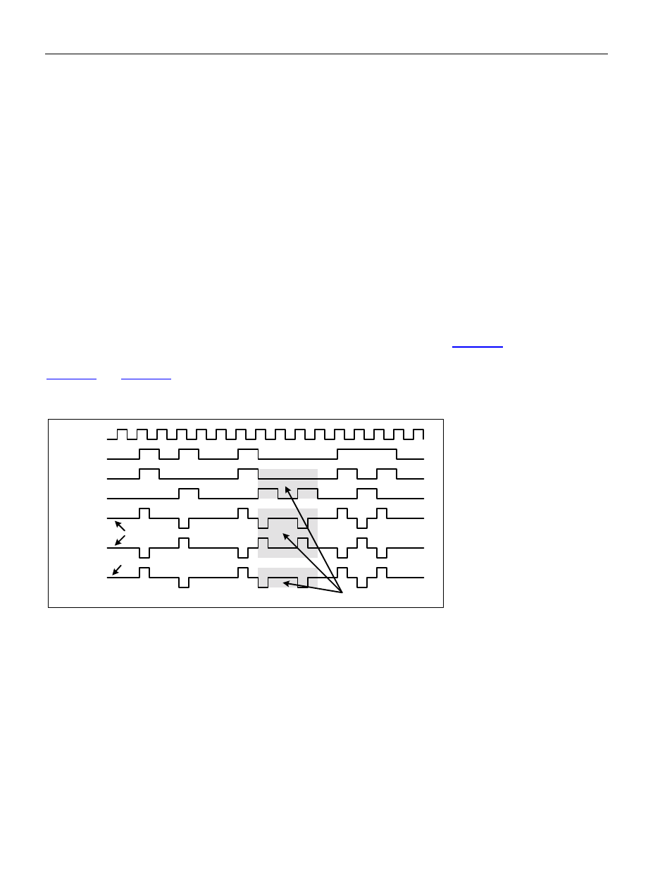
There is no suggested time alignment between the TXP, TXN and TX LINE signals and the TLCLK clock signal.
The TX DATA signal is not a readily available signal, it is meant to represent the data value of the other signals.
The TXP and TXN signals are only available when the line is in B3ZS/HDB3 or AMI mode and the LIU is enabled.
The TPOS, TNEG and TLCLK signals are only available when the line is in B3ZS/HDB3 or AMI mode and the
transmit line pins are enabled. The TPOS, TNEG and TLCLK pins can be enabled at the same as the LIU is
enabled.
The TPOS and TNEG signals change a small delay after the positive edge of the reference clock if the clock pin is
not inverted, otherwise they change after the negative edge. The TLCLK clock pin is the clock reference typically
used for the TPOS and TNEG signals, but they can be time referenced to the TCLKI, TCLKO, RLCLK or RCLKO
clock pins. The TPOS and TNEG pins can be inverted, but the polarity of TXP and TXN can not be inverted.
TXP and TXN are differential analog output pins. They are biased around ½ VDD and pulse above and below the
bias voltage by about 1 Volt. These signals are connected to the windings of a 1:2 step down transformer and the
other winding of the transformer creates the TX LINE signal. The TX LINE signal is a bipolar signal that pulses
about 1 Volt positive and 1 Volt negative above and below ground (0 volts). See
for a diagram of the
external connections.
show the relationship between the analog and the digital outputs.
Figure 7-1. Tx Line IO B3ZS Functional Timing Diagram
TLCLK
TPOS
TNEG
(TX DATA)
B3ZS CODEWORD
(TX LINE)
+
-
TXP
TXN
V
V
B
B
B
V
B
V
0 V
BIAS V