Hdlc receive side register map, Register bit descriptions, Table 11-17. receive side hdlc register map – Rainbow Electronics DS3170 User Manual
Page 159: Hdlc.rcr
DS3170 DS3/E3 Single-Chip Transceiver
159 of 233
Bit 2: Transmit FIFO Full Interrupt Enable (TFFIE) – This bit enables an interrupt if the TFFL bit is set and the bit
in
.PSRIE[4:1] that corresponds to this port is set.
0 = interrupt disabled
1 = interrupt enabled
Bit 1: Transmit FIFO Empty Interrupt Enable (TFEIE) – This bit enables an interrupt if the TFEL bit is set and the
bit in
.PSRIE[4:1] that corresponds to this port is set.
0 = interrupt disabled
1 = interrupt enabled
Bit 0: Transmit HDLC Data Available Interrupt Enable (THDAIE) – This bit enables an interrupt if the THDAL bit
is set and the bit in
.PSRIE[4:1] that corresponds to this port is set.
0 = interrupt disabled
1 = interrupt enabled
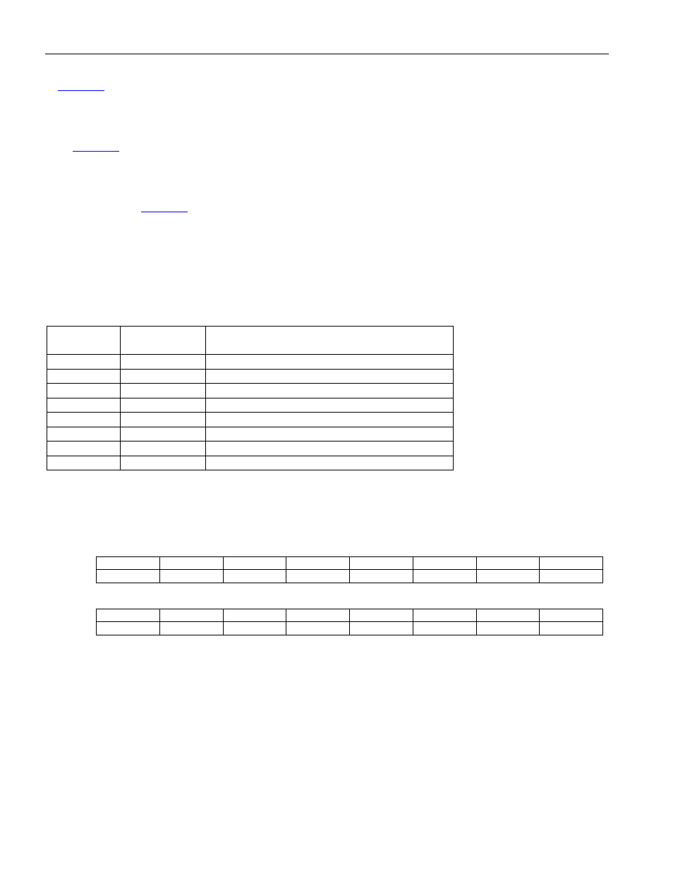
11.6.2 HDLC Receive Side Register Map
The receive side utilizes five registers.
Table 11-17. Receive Side HDLC Register Map
Address
Register
Register Description
0B0h HDLC.RCR
HDLC Receive Control Register
0B2h --
Unused
0B4h HDLC.RSR
HDLC Receive Status Register
0B6h HDLC.RSRL
HDLC Receive Status Register Latched
0B8h HDLC.RSRIE
HDLC Receive Status Register Interrupt Enable
0BAh --
Unused
0BCh HDLC.RFDR
HDLC Receive FIFO Data Register
0BEh --
Unused
11.6.2.1 Register Bit Descriptions
Register Name:
HDLC.RCR
Register Description:
HDLC Receive Control Register
Register Address:
0B0h
Bit
# 15 14 13 12 11 10 9 8
Name
-- -- --
RDAL4
RDAL3 RDAL2 RDAL1 RDAL0
Default
0 0 0 0 1 0 0 0
Bit
# 7 6 5 4 3 2 1 0
Name
-- -- -- --
RBRE
RDIE
RFPD
RFRST
Default
0 0 0 0 0 0 0 0
Bits 12 to 8: Receive HDLC Data Available Level (RDAL[4:0]) – These five bits indicate the minimum number of
eight byte groups that must be stored (contain data) in the Receive FIFO before HDLC data is considered to be
available (RHDA=1). For example, a value of 21 (15h) results in HDLC data being available when the Receive
FIFO contains 168 (A8h) bytes or more.
Bit 3: Receive Bit Reordering Enable (RBRE) – When 0, bit reordering is disabled (The first bit received is in the
LSB of the Receive FIFO Data byte RFD[0]). When 1, bit reordering is enabled (The first bit received is in the MSB
of the Receive FIFO Data byte RFD[7]).
Bit 2: Receive Data Inversion Enable (RDIE) – When 0, the incoming data is directly passed on for packet
processing. When 1, the incoming data is inverted before being passed on for packet processing.
Bit 1: Receive FCS Processing Disable (RFPD) – When 0, FCS processing is performed (the packets have an
FCS appended). When 1, FCS processing is disabled (the packets do not have an FCS appended).