Framer data path ac characteristics, Ramer, Ac c – Rainbow Electronics DS3170 User Manual
Page 220: Haracteristics, Table 17-1. framer interface timing, Table 17-2. system port interface timing, Ied in, Table 17-1, 1 framer data path ac characteristics
DS3170 DS3/E3 Single-Chip Transceiver
220 of 233
17.1 Framer Data Path AC Characteristics
All AC timing characteristics are specified with a 25 pF capacitive load on all output pins, V
IH
= 2.4V and V
IL
= 0.8V.
The voltage threshold for all timing measurements is VDD/2. The generic timing definitions shown in in
and
apply to this interface
.
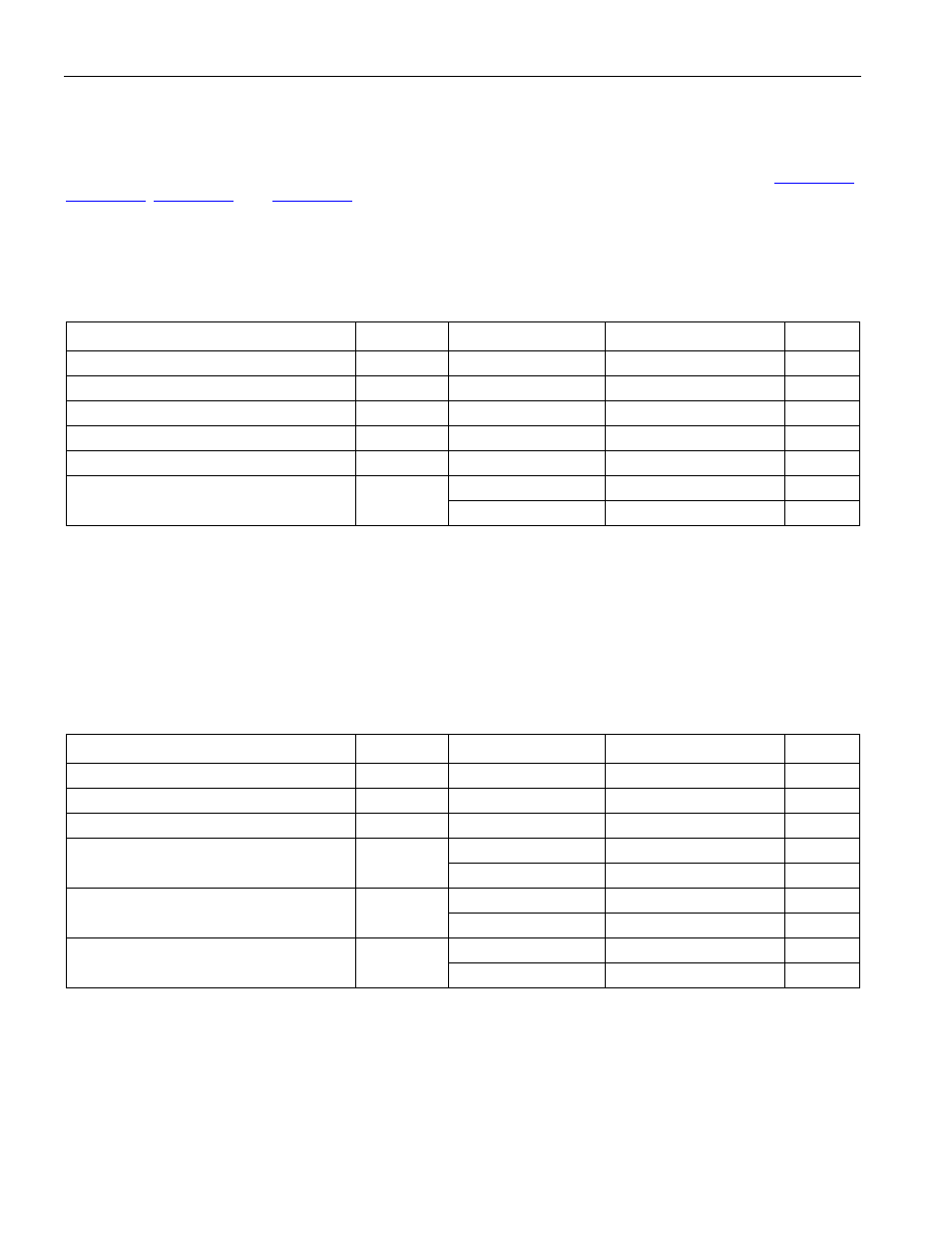
Table 17-1. Framer Interface Timing
(V
DD
= 3.3V
±5%, T
j
= -40°C to +125°C.)
PARAMETER SYMBOL
CONDITIONS
MIN
TYP
MAX
UNITS
CLK Frequency
f1(1/t1)
(Note 1)
52
MHz
CLK Clock Duty Cycle (t2/t1)
t2/t1
(Note 2)
40
50
60
%
CLK Rise or Fall Times (20% to 80%)
t3
(Note 2)
4
ns
DIN to CLK Setup Time
t5
(Note 3)
4
ns
CLK to DIN Hold Time
t6 (Note
3)
0 ns
(Note 4)
2
10
ns
CLK to DOUT Delay
t7
(Note
5)
2 8 ns
Note 1:
Any mode, TCLKI, RLCLK input clocks.
Note 2:
Any mode, TCLKI, RLCLK input clocks.
Note 3:
RLCLK clock input to RPOS/RDAT, RNEG/RLCV inputs.
Note 4:
TCLKI, RLCLK clock inputs to TPOS/TDAT, TNEG outputs.
Note 5:
TLCLKn, TCLKO, RCLKO clock outputs to TPOS/TDAT, TNEG outputs.
Table 17-2. System Port Interface Timing
(V
DD
= 3.3V
±5%, T
j
= -40°C to +125°C.)
PARAMETER SYMBOL
CONDITIONS
MIN
TYP
MAX
UNITS
CLK Frequency
f1(1/t1)
(Note 1)
52
MHz
CLK Clock Duty Cycle (t2/t1)
t2/t1
(Note 2)
40
50
60
%
CLK Rise or Fall times (20% to 80%)
t3
(Note 2)
4
ns
(Note 3)
3
ns
DIN to CLK Setup Time
t5
(Note 4)
7
ns
(Note 3)
1
ns
CLK to DIN Hold Time
t6
(Note 4)
1
ns
(Note 5)
2
10
ns
CLK to DOUT Delay
t7
(Note
6)
2 8 ns
Note 1:
Any mode, TCLKI, RLCLK input clocks.
Note 2:
Any mode, TCLKI, RLCLK input clocks.
Note 3:
TCLKI, RLCLK clock inputs to TSOFI, TSER inputs.
Note 4:
TCLKO, RCLKO clock outputs to TSOFI, TSER inputs.
Note 5:
TCLKI, RLCLK clock input to TSOFO/TDEN, RSER, RSOFO/RDEN outputs.
Note 6:
TCLKO, RCLKO clock output to TSOFO/TDEN, RSER, RSOFO/RDEN outputs.