Figure 7-13, Figure 7-15 – Rainbow Electronics DS3170 User Manual
Page 42

DS3170 DS3/E3 Single-Chip Transceiver
42 of 233
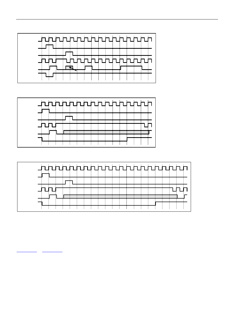
Figure 7-13. DS3 Framed Mode Transmit Serial Interface Pin Timing
TCLKO or
TCLKI
DS3 TSER
DS3 TDEN
TSOFO
DS3 TGCLK
TSOFI
TSER DATA IS OVERWRITTEN WITH OH
6
7
8
9
10 11 12 13
1
2
3
4
5
14 15
Figure 7-14. E3 G.751 Framed Mode Transmit Serial Interface Pin Timing
E3 TSER
E3 TDEN
E3 TGCLK
TCLKO or
TCLKI
TSOFO
TSOFI
TSER DATA IS OVERWRITTEN WITH OH
6
7
8
9
10 11 12 13
1
2
3
4
5
14 15
Figure 7-15. E3 G.832 Framed Mode Transmit Serial Interface Pin Timing
E3 TSER
E3 TDEN
E3 TGCLK
TCLKO or
TCLKI
TSOFO
TSER DATA IS OVERWRITTEN WITH OH
TSOFI
6
7
8
9
10 11 12 13
1
2
3
4
5
14 15 16 17 18 19 20
7.3.3.2 DS3/E3 Framed Mode Receive Serial Interface Pin Functional Timing
The RSER signal has the DS3 or E3 payload as well as the DS3 or E3 overhead bits. The RDEN signal is used to
enable external logic for payload processing and will be high during the DS3 or E3 payload bits and low during the
DS3 or E3 overhead bits. The RGCLK signal can also be used to clock only the DS3 or E3 payload bits into
external logic since the clock is stopped during the DS3 or E3 overhead bits. The RSOFO signal marks the first
overhead bit of the DS3 or E3 frame.
show the relationship between the receive serial interface pins.
