Sources of clock output pin signals, Table 9-1. liu enable table – Rainbow Electronics DS3170 User Manual
Page 57
DS3170 DS3/E3 Single-Chip Transceiver
57 of 233
9.2.2 Sources of Clock Output Pin Signals
The clock output pins can be sourced from many clock sources. The clock sources are the transmit input clocks pin
(TCLKI), the receive clock input pin (RLCLK), the recovered clock in the receive LIU, and the clock signals in the
clock rate adapter circuit (CLAD). The default clock source for the receive logic is the RLCLK pin if the LIU is
disabled; otherwise the default clock is sourced from the Rx LIU clock when the RX LIU is enabled. The default
clock source for the transmit logic is the CLAD clocks.
The LIU is enabled based on the line mode bits(LM[2:0]) (see
). The bits LM[2:0], LBM[2:0], LOOPT and
CLADC are located in the port configuration registers. LIUEN is not a register bit; it is a variable based on the line
mode bits.
decodes the LM bits for LiUEN selection.
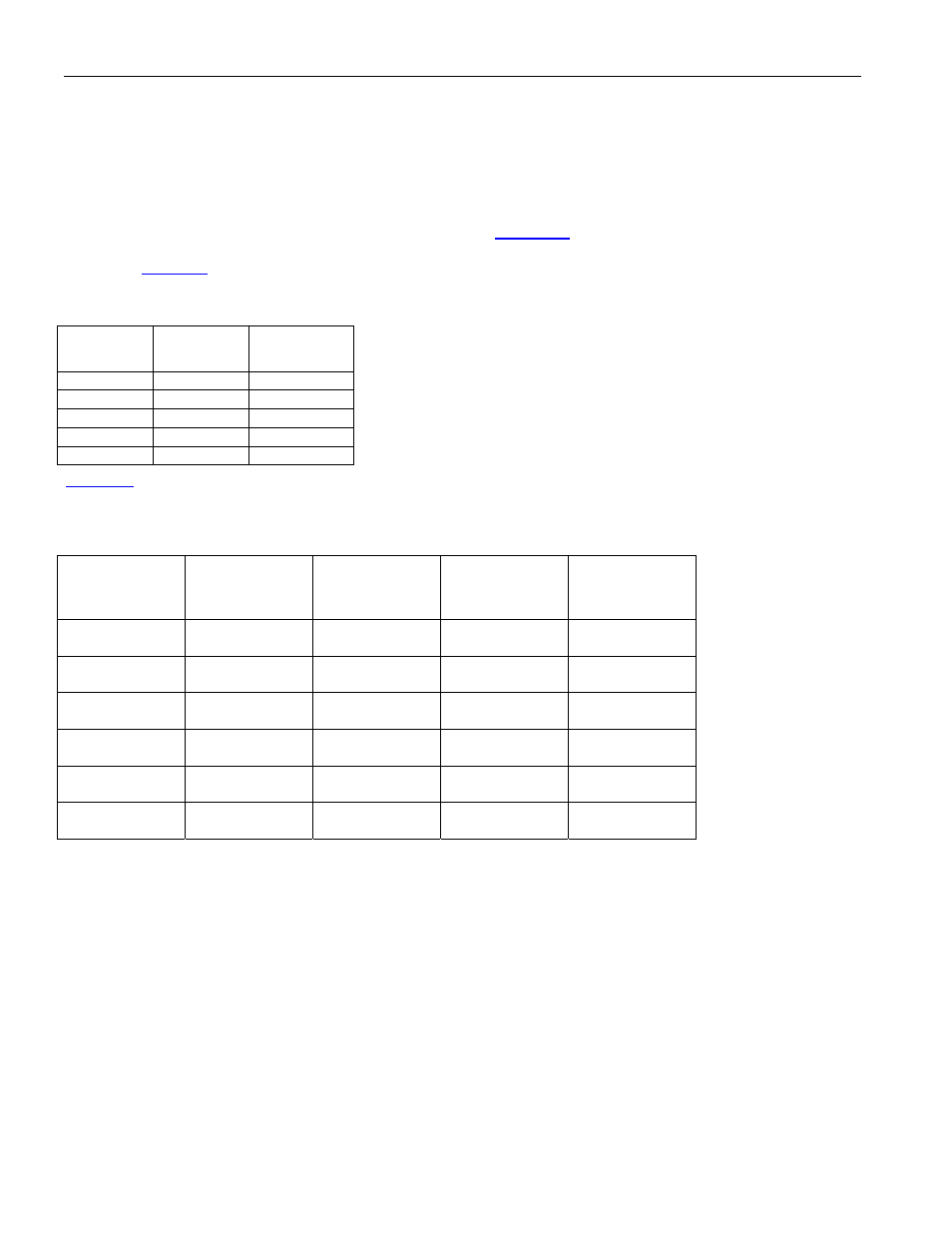
Table 9-1. LIU Enable Table
LM[2:0] LIUEN
LIU
STATUS
000 0
Disabled
001 1
Enabled
010 1
Enabled
011 1
Enabled
1XX 0
Disabled
identifies the framer clock source and the line clock source depending on the mode that the device is
configured. Putting the device in loopback will typically mux in a different clock than the normal clock source.
Table 9-2. All Possible Clock Sources Based on Mode and Loopback
MODE LOOPBACK
Rx FRAMER
CLOCK
SOURCE
Tx FRAMER
CLOCK
SOURCE
Tx LINE
CLOCK
SOURCE
Loop Timed
Any
RLCLK or
RXLIU
Same as RX
Same as Rx
Normal None
RLCLK or
RXLIU
TCLKI or
CLAD
Same as Tx
Normal LLB
RLCLK or
RXLIU
TCLKI or
CLAD
Same as Rx
Normal PLB
RLCLK or
RXLIU
Same as RX
Same as Rx
Normal
DLB
Same as Tx
TCLKI or
CLAD
Same as Tx
Normal
LLB and DLB
Same as Tx
TCLKI or
CLAD
RLCLK or
RXLIUn