Clock structures on signal io pins – Rainbow Electronics DS3170 User Manual
Page 62
DS3170 DS3/E3 Single-Chip Transceiver
62 of 233
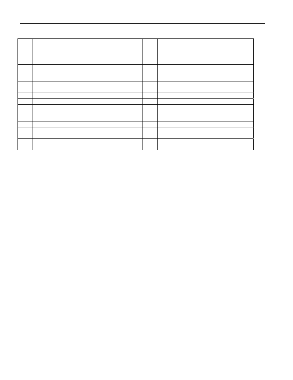
Table 9-9. Receive Framer Pin Signal Timing Source Select
LOOP
T
LBM[2:0]
LIUEN
CLADC
RFTS
VALID TIMING TO THESE CLOCK PINS
1
XXX
X
X
0
RCLKO, TLCLK, TCLKO
1
XXX
0 X 1
RLCLK
1
XXX
1
X
1
No valid timing to any input clock pin
0
PLB (011) or DLB (100) or ALB
(001)
0 X 0
RCLKO,
TLCLK,
TCLKO
0
PLB (011) or DLB (100)
1
X
0
RCLKO, TLCLK, TCLKO
0
DLB&LLB (110)
X
X
0
RCLKO, TCLKO
0
LLB (010)
X
X
0
RCLKO, TLCLK
0
not LLB, DLB or PLB (00X)
X
X
0
RCLKO
0
DLB (100) or LLB & DLB (110)
X
0
1
No valid timing to any input clock pin
0
DLB (100) or LLB & DLB (110)
X
1
1
TCLKI
0
not DLB (100) and
not LLB & DLB (110)
0 X 1
RLCLK
0
not DLB (100) and
not LLB & DLB (110)
1
X
1
No valid timing to any input clock pin
9.2.4 Clock Structures On Signal IO Pins
The signals on the input pins (TSOFI, TSER) can be used with any of the clock pins for setup/hold timing on clock
input and output pins. There will be a flop at each input whose clock is connected to the signal from the input or
output clock source pins with as little delay as possible from the signal on the clock IO pins. This means using the
input clock signal before the delays of the internal clock tree to clock the input signals, and using the output clock
signals used to drive the output clock pins to clock the input signals.
The signals on the output pins (TPOS/TDAT, TNEG, TSOFO/TDEN, RSER, RSOFO/RDEN) can be with any of the
clock sources for delay timing. There will be a flop at each output whose clock is connected to the signal from the
input or output clock source pins with as little delay as possible from the signal on the clock IO pins. This means
using the input clock signal before the delays of the internal clock tree to clock the input signals, and using the
output clock signals used to drive the output clock pins to clock the input signals.