Rainbow Electronics DS3170 User Manual
Page 44
DS3170 DS3/E3 Single-Chip Transceiver
44 of 233
expected. If the BURST bit is not set, each data byte will be followed by the control byte(s) for the next access.
Additionally,
CS may also be de-asserted between accesses when CPHA =1. In the case, any BURST access is
terminated, and the next byte received when
CS is re-asserted will be a control byte.
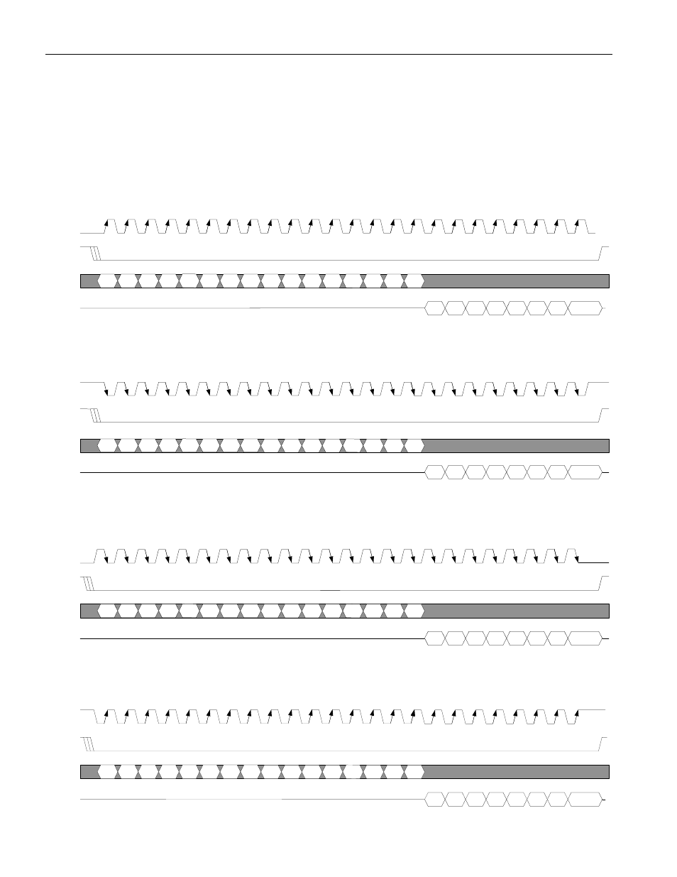
The following diagrams describe the functionality of the SPI port for the four combinations of SPI_CPOL and
SPI_CPHA. They indicate the clock edge that samples the data and the level of the clock during no-transfer events
(high or low). Since the SPI port of the DS3170 acts as a slave device, the master device provides the clock. The
user must configure the SPI_CPOL and SPI_CPHA pins to describe which type of clock that the master device is
providing.
Figure 7-19. SPI Serial Port Access For Read Mode, SPI_CPOL=0, SPI_CPHA = 0
1
A7
A13
A12
A11
A10
A9
A8
D7
D6
D5
D4
D3
D2
D1
D0
LSB
MSB
LSB
MSB
SCK
CS*
MOSI
MISO
B
A6
A5
A4
A3
A2
A1
LSB
MSB
A0
Figure 7-20. SPI Serial Port Access For Read Mode, SPI_CPOL = 1, SPI_CPHA = 0
SCK
CS*
1
A7
A13
A12
A11
A10
A9
A8
D7
D6
D5
D4
D3
D2
D1
D0
LSB
MSB
LSB
MSB
MOSI
MISO
B
A6
A5
A4
A3
A2
A1
LSB
MSB
A0
Figure 7-21. SPI Serial Port Access For Read Mode, SPI_CPOL = 0, SPI_CPHA = 1
SCK
CS*
1
A7
A13
A12
A11
A10
A9
A8
D7
D6
D5
D4
D3
D2
D1
D0
LSB
MSB
LSB
MSB
MOSI
MISO
B
A6
A5
A4
A3
A2
A1
LSB
MSB
A0
Figure 7-22. SPI Serial Port Access For Read Mode, SPI_CPOL = 1, SPI_CPHA = 1
SCK
CS*
1
A7
A13
A12
A11
A10
A9
A8
D7
D6
D5
D4
D3
D2
D1
D0
LSB
MSB
LSB
MSB
MOSI
MISO
B
A6
A5
A4
A3
A2
A1
LSB
MSB
A0