Figure 7-31. 16-bit mode without byte swap, Figure 7-32b 16-bit mode with byte swap, Figure 7-31 – Rainbow Electronics DS3170 User Manual
Page 48: Figure 7-32
DS3170 DS3/E3 Single-Chip Transceiver
48 of 233
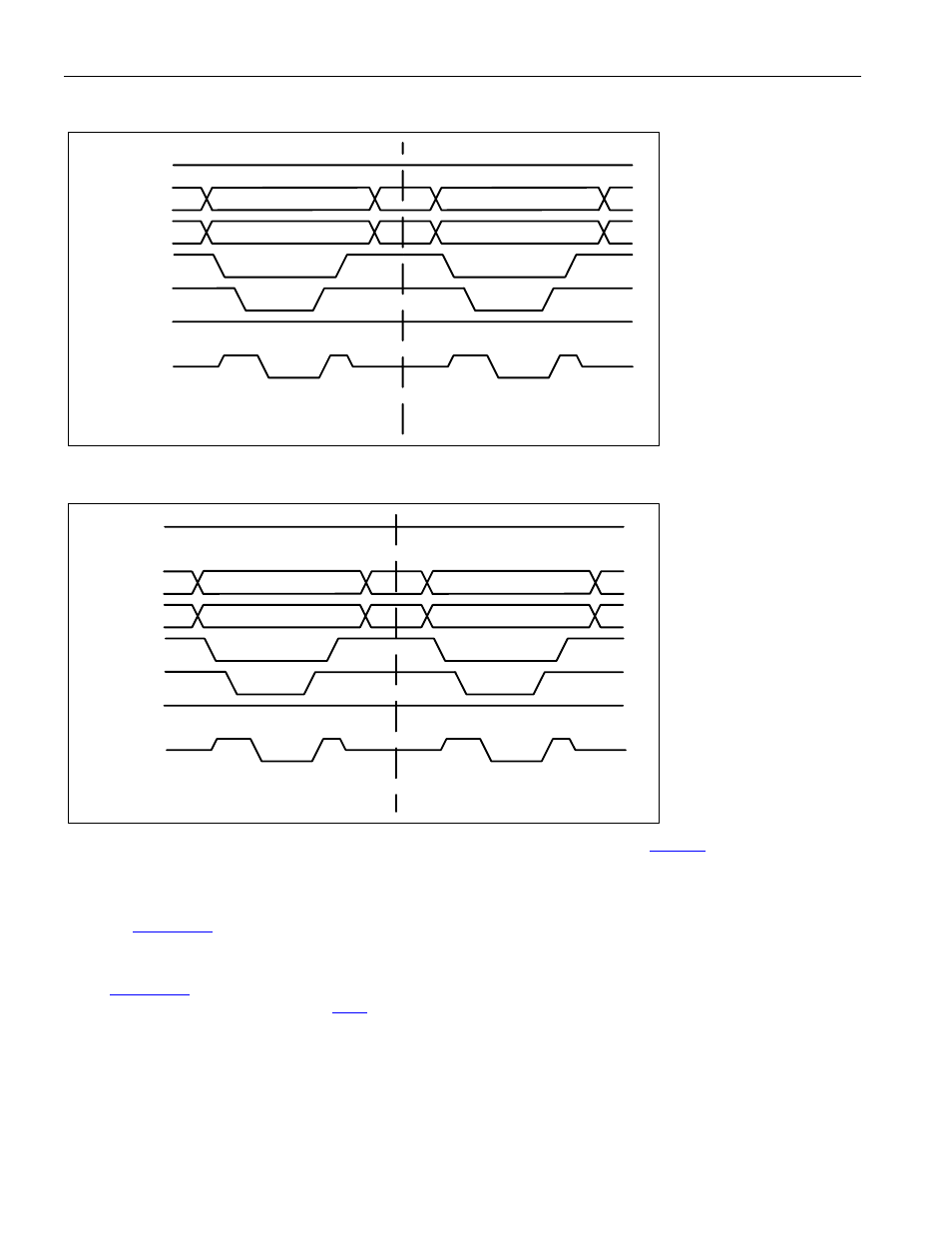
Figure 7-31. 16-Bit Mode without Byte Swap
0x1234
0x5678
Note: Address 0x2B0 = 0x1234
0x2B2 = 0x5678
0x2B0
0x2B2
D[15:0]
A[10:1]
A[0]/BSWAP
Z
Z
Z
Z
RD
WR
CS
RDY
Figure 7-32b 16-Bit Mode with Byte Swap
0x3412
0x7856
Note: Address 0x2B0 = 0x1234
0x2B2 = 0x5678
0x2B0
0x2B2
D[15:0]
A[10:1]
A[0]/BSWAP
Z
Z
Z
Z
RD
WR
CS
RDY
Clearing status latched registers on a read or write access is selectable via the
.LSBCRE register bit.
Clearing on read clears all bits in the register, while the clear on write clears only those bits which are written with a
‘1’ when the user writes to the status latched register.
To use the Clear on Read method, the user must only read the status latched register. All bits are set to zero after
the read.
shows a read of a status latched register and another read of the same register verifying the
register has cleared.
To use the Clear on Write method, the user must write the register with ones in the bit locations that he desires to
clear.
shows a read, a write, and then a subsequent read revealing the results of clearing of the bits,
which he wrote a ‘1.’ See also Section