Rainbow Electronics DS3131 User Manual
General description, Applications, Features
1 of 174
112002
Note: Some revisions of this device may incorporate deviations from published specifications known as errata. Multiple revisions of any device
may be simultaneously available through various sales channels. For information about device errata, click here:
GENERAL DESCRIPTION
The DS3131 bit-synchronous (BoSS) HDLC
controller can handle up to 40 channels of high-
speed, unchannelized, bit-synchronous HDLC.
The on-board DMA has been optimized for
maximum flexibility and PCI bus efficiency to
minimize host processor intervention in the data
path. Diagnostic loopbacks and an on-board
BERT remove the need for external components.
APPLICATIONS
Routers
xDSL Access Multiplexers (DSLAMs)
Clear-Channel (unchannelized) T1/E1
Clear-Channel (unchannelized) T3/E3
SONET/SDH Path Overhead Termination
High-Density V.35 Terminations
High-Speed Links such as HSSI
FEATURES
40 Timing Independent Ports
40 Bidirectional HDLC Channels
Each Port Can Operate Up to 52Mbps
Up to 132Mbps Full-Duplex Throughput
On-Board Bit Error-Rate Tester (BERT)
Diagnostic Loopbacks in Both Directions
Local Bus Supports PCI Bridging
33MHz 32-Bit PCI Interface
Full Suite of Driver Code
Features continued on page 6.
ORDERING INFORMATION
PART TEMP
RANGE PIN-PACKAGE
DS3131
0°C to +70°C
272 PBGA
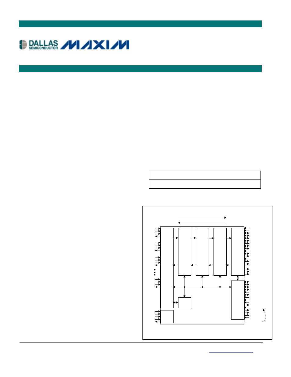
FUNCTIONAL DIAGRAM
PIN NAMES IN ( )
ARE ACTIVE WHEN
THE DEVICE IS IN
THE MOT MODE
(i.e., LIM = 1).
RC2
RD2
TC2
TD2
JTDO
PCLK
PAD[31:0]
PRST
PCBE[3:0]
PPAR
PFRAME
PIRDY
PTRDY
PSTOP
PIDSEL
PDEVSEL
PREQ
PGNT
PPERR
PSERR
RC39
RD39
TC39
TD39
RC0
RD0
TC0
TD0
RC1
RD1
TC1
TD1
PXAS
PXDS
PXBLAST
JTRST
JTDI
JTMS
JTCLK
LA[19:0]
LD[15:0]
LWR(LR/W)
LRD(LDS)
LIM
LINT
LRDY
LMS
LCS
LHOLD(
LBR)
LHLDA(
LBG)
LBGACK
LCLK
LBHE
JTAG TEST
ACCESS
(SECT. 12)
LO
CA
L B
U
S
B
LO
C
K
(SEC
T
. 1
1)
LAYER
1
BL
O
C
K (
SEC
T
. 6
)
40-
B
IT
S
Y
NCHRO
NO
U
S
HDLC CO
NT
R
O
LLE
RS
(
S
E
C
T
. 7)
FI
FO
B
LOC
K
(
S
E
C
T.
8
)
D
M
A BL
O
C
K (S
EC
T
. 9
)
PC
I BL
O
C
K (S
EC
T
. 1
0)
BERT
(SECT. 6)
RECEIVE DIRECTION
TRANSMIT DIRECTION
INTERNAL CONTROL BUS
LBPXS
DS3131
DS3131 BoSS
40-Port, Unchannelized
Bit-Synchronous HDLC
www.maxim-ic.com
DEMO KIT AVAILABLE
Document Outline
- MAIN FEATURES
- DETAILED DESCRIPTION
- SIGNAL DESCRIPTION
- MEMORY MAP
- Introduction
- General Configuration Registers (0xx)
- Receive Port Registers (1xx)
- Transmit Port Registers (2xx)
- Receive HDLC Control Registers (3xx)
- TRANSMIT HDLC CONTROL REGISTERS (4xx)
- BERT Registers (5xx)
- Receive DMA Registers (7xx)
- Transmit DMA Registers (8xx)
- FIFO Registers (9xx)
- PCI Configuration Registers for Function 0 (PIDSEL/Axx)
- PCI Configuration Registers for Function 1 (PIDSEL/Bxx)
- GENERAL DEVICE CONFIGURATION AND STATUS/INTERRUPT
- LAYER 1
- HDLC
- FIFO
- DMA
- PCI BUS
- LOCAL BUS
- JTAG
- AC CHARACTERISTICS
- MECHANICAL DIMENSIONS
- APPLICATIONS