Port.cr3, Port – Rainbow Electronics DS3170 User Manual
Page 137
DS3170 DS3/E3 Single-Chip Transceiver
137 of 233
Register Name:
PORT.CR3
Register Description:
Port Control Register 3
Register Address:
044h
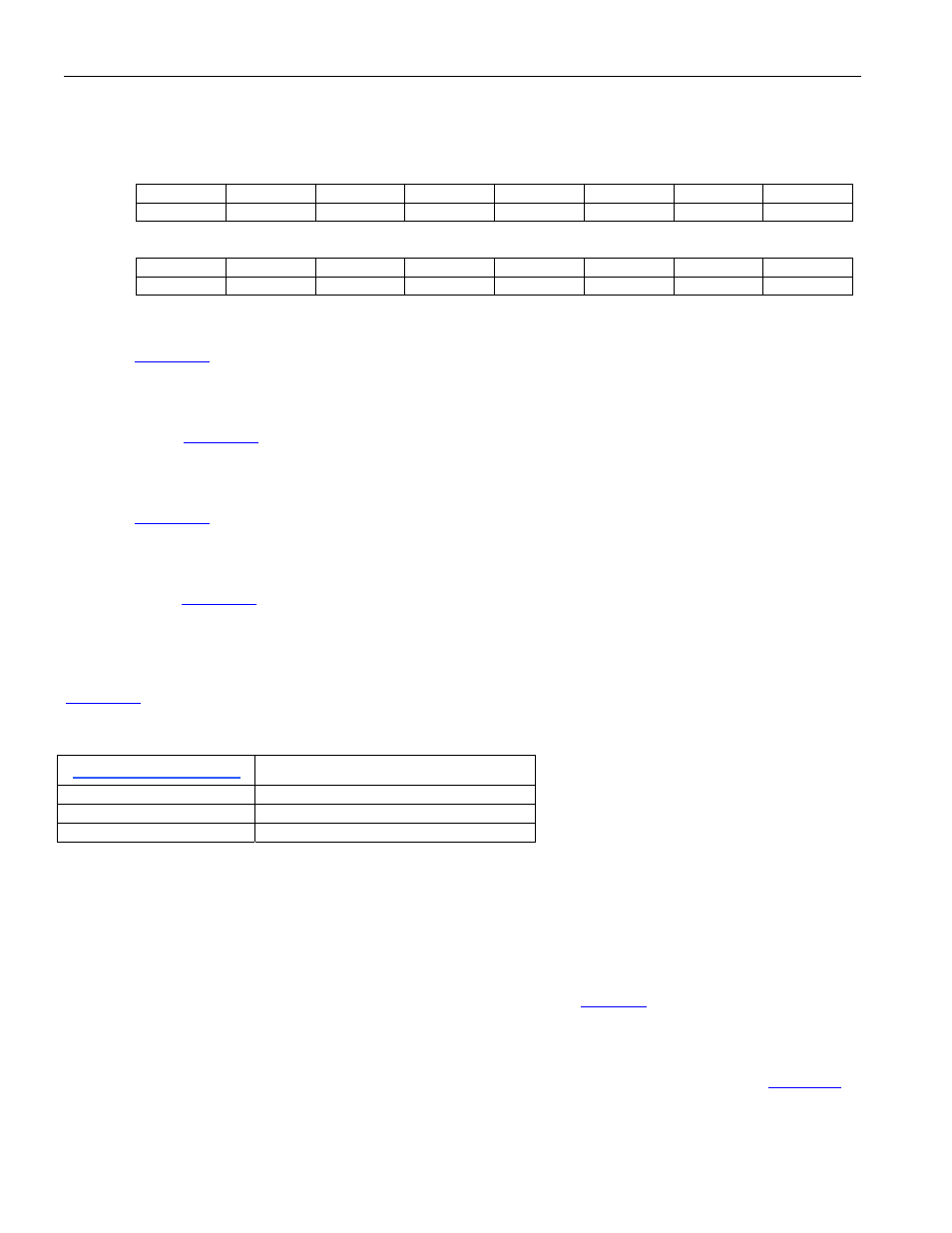
Bit
# 15 14 13 12 11 10 9 8
Name -- --
RCLKS
RSOFOS
RESERVED
TCLKS TSOFOS
RESERVED
Default
0 0 0 0 0 0 0 0
Bit
# 7 6 5 4 3 2 1 0
Name P8KRS1
P8KRS0
P8KREF
LOOPT CLADC RFTS TFTS TLTS
Default
0 0 0 0 0 0 0 0
Bit 13: Receive Clock Output Select (RCLKS). This bit is used to select the function of the RGCLK / RCLKO
pins. See
0 = Selects the RGCLK signal, or the drive low pin function.
1 = Selects RCLKO signal.
Bit 12: Receive Start Of Frame Output Select (RSOFOS). This bit is to select the function of the RSOFO /
RDEN pins. See
0 = Selects RDEN signal.
1 = Selects RSOFO signal.
Bit 10: Transmit Clock Output Select (TCLKS). This bit is used to select the function of the TGCLK / TCLKO
pins. See
0 = Selects TGCLK signal.
1 = Selects TCLKO signal.
Bit 9: Transmit Start Of Frame Output Select (TSOFOS). This bit is used to select the function of the TSOFO /
TDEN pins. See
0 = Selects TDEN signal.
1 = Selects TSOFO signal.
Bits 7 to 6: Port 8 kHz Reference Source Select (P8KRS[1:0]). This bit selects the source of the 8 kHz
reference from the port sources. The 8K reference for this port can be used as the global 8K reference source. See
Table 9-13. Port 8 kHz Reference Source Table
PORT.CR3.P8KRS[1:0]
SOURCE
11
Internal transmit framer clock
Bit 5: PORT 8 kHz Reference Source (P8KREF). This bit selects the source of the 8 kHz reference for one
second timer.
0 = 8 kHz reference from global source
1 = 8 kHz reference from port’s selected source
Bit 4: LOOP Time Enable (LOOPT). When this bit is set, the port is in loop time mode. The transmit clock is set
to the receive clock from the RLCLK pin or the recovered clock from the LIU or the CLAD clock
and the TCLKI pin
is not used. This function of this bit is conditional on other control bits. See
for more details.
0 = Normal transmit clock operation
1 = Transmit using the receive clock
Bit 3: CLAD Transmit Clock Source Control (CLADC). This bit is used to enable the CLAD clocks as the
source of the internal transmit clock. This function of this bit is conditional on other control bits. See
for
more details.
0 = Use CLAD clocks for the transmit clock as appropriate
1 = Do not use CLAD clocks for the transmit clock – (if no loopback is enabled, TCLKI is the source)