Rainbow Electronics MAX9489 User Manual
Max9489 multiple-output network clock generator, General description, Applications
General Description
The MAX9489 clock generator provides multiple clock
outputs, ideal for network routers. The MAX9489 pro-
vides 15 buffered clock outputs, each independently
programmable to any of 10 individual frequencies:
133MHz, 125MHz, 100MHz, 83MHz, 80MHz, 66MHz,
62.5MHz, 50MHz, 33MHz, or 25MHz. All of the outputs
are single-ended LVCMOS. The MAX9489 is controlled
through its I
2
C™ interface.
At power-up, the frequency of output CLK1 is set by the
tri-level input SEL to 100MHz, 125MHz, or 133MHz,
while all other outputs are logic low. All outputs are then
programmable to any available frequency through the
I
2
C interface. Additionally, all output frequencies are
adjustable up or down, by a margin of 5% or 10%,
through the I
2
C interface.
The MAX9489 requires a 25MHz reference that can be
either a crystal or an external clock signal. The
MAX9489 requires a +3.0V to +3.6V power supply and
is available in a 32-pin thin QFN package with an
exposed pad for heat removal.
Applications
Network Routers
Telecom/Networking Equipment
Storage Area Networks/Network Attached
Storage
Features
♦ 15 LVCMOS Outputs with 10 Independently
Programmable Frequencies: 133MHz, 125MHz,
100MHz, 83MHz, 80MHz, 66MHz, 62.5MHz, 50MHz,
33MHz, and 25MHz
♦ 25MHz Crystal or Clock Input Reference
♦ Programmable Through I
2
C Interface
♦ Programmable Output Frequency Margin of ±5%
or ±10%
♦ Pin-Selectable Power-Up Frequency for CLK1
Output: 100MHz, 125MHz, or 133MHz
♦ Low Output Period Jitter: < 48ps
RMS
♦ Output-to-Output Skew < 200ps
♦ Available in 32-Lead, 5mm x 5mm x 0.8mm,
Thin QFN Package
♦ Operates from +3.0V to +3.6V Power Supply
♦ Power Dissipation 450mW (typ)
♦ Extended Temperature Range: -40°C to +85°C
MAX9489
Multiple-Output Network Clock Generator
________________________________________________________________ Maxim Integrated Products
1
Ordering Information
19-3385; Rev 0; 8/04
For pricing, delivery, and ordering information, please contact Maxim/Dallas Direct! at
1-888-629-4642, or visit Maxim’s website at www.maxim-ic.com.
PART
TEMP RANGE
PIN-PACKAGE
MAX9489ETJ
-40
°C to +85°C
32 Thin QFN-EP*
5mm x 5mm x 0.8mm
GND
1
SCL
2
SDA
3
SEL
4
AV
DD
5
X1
6
X2
7
AGND
8
V
DD
24
CLK12
23
CLK11
22
CLK10
21
V
DD
20
CLK9
19
CLK8
18
CLK7
17
CLK1
9
CLK2
10
CLK3
11
V
DD
12
CLK4
13
CLK5
14
CLK6
15
V
DD
16
V
DD
32
SA1
31
SA0
30
GND
29
V
DD
28
CLK15
27
CLK14
26
CLK13
25
MAX9489
THIN QFN-EP
TOP VIEW
EXPOSED PAD (GND)
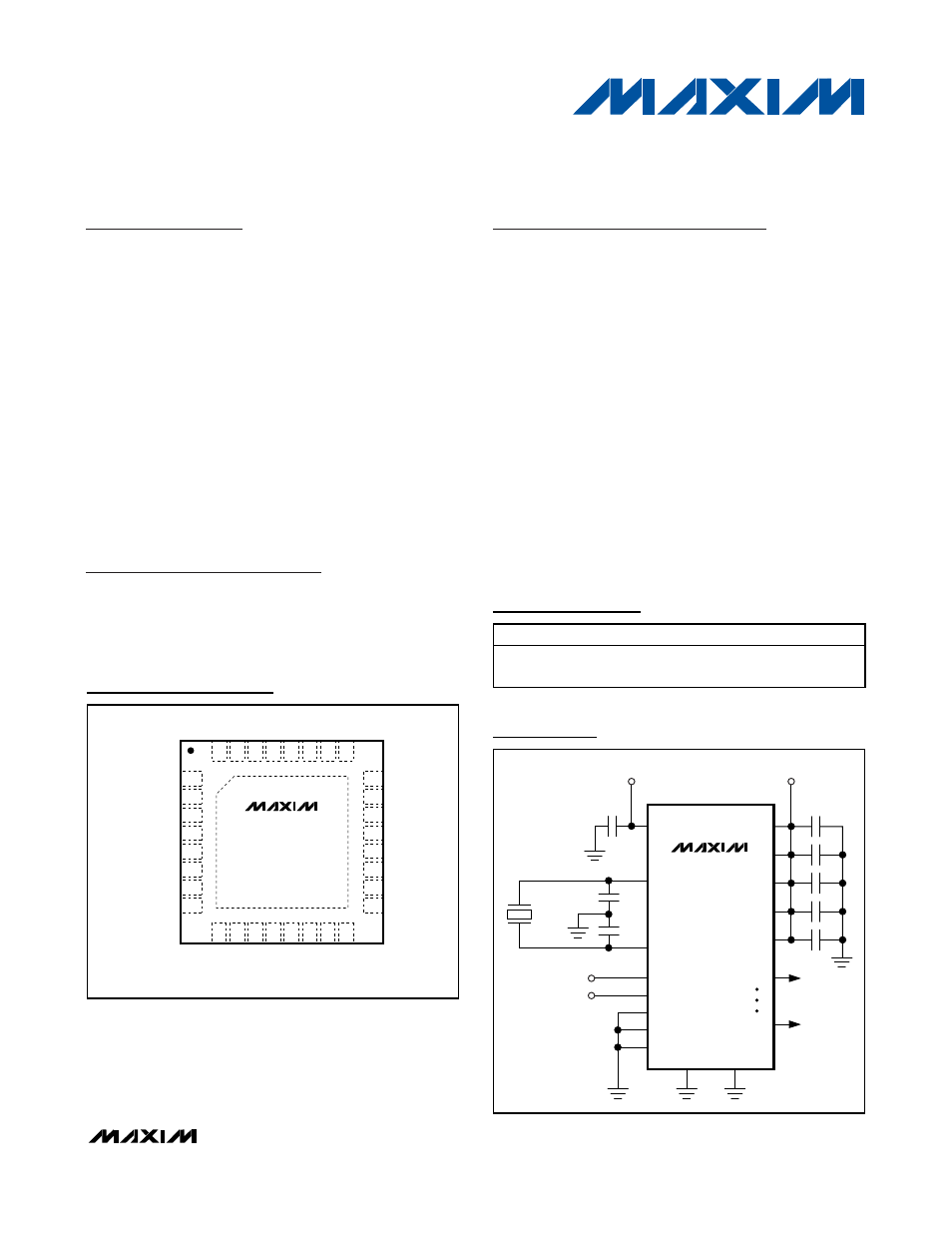
Pin Configuration
MAX9489
25MHz
10pF
10pF
X1
AV
DD
X2
SDA
0.1
µF
SCL
SA0
SA1
SEL
AGND
GND
CLK15
CLK1
V
DD
V
DD
V
DD
V
DD
V
DD
+3.3V
+3.3V
SERIAL
INTERFACE
CLOCK
OUTPUTS
0.1
µF x 5
Typical Operating Circuit
I
2
C is a trademark of Philips Corp.
Purchase of I
2
C components of Maxim Integrated Products, Inc.,
or one of its sublicensed Associated Companies, conveys a
license under the Philips I
2
C Patent Rights to use these compo-
nents in an I
2
C system, provided that the system conforms to the
I
2
C Standard Specification as defined by Philips.
*EP = Exposed pad.