Clocks, Line clock modes, Loop timing enabled – Rainbow Electronics DS3170 User Manual
Page 55: Locks, Figure 9-1. interrupt structure, 2 clocks
DS3170 DS3/E3 Single-Chip Transceiver
55 of 233
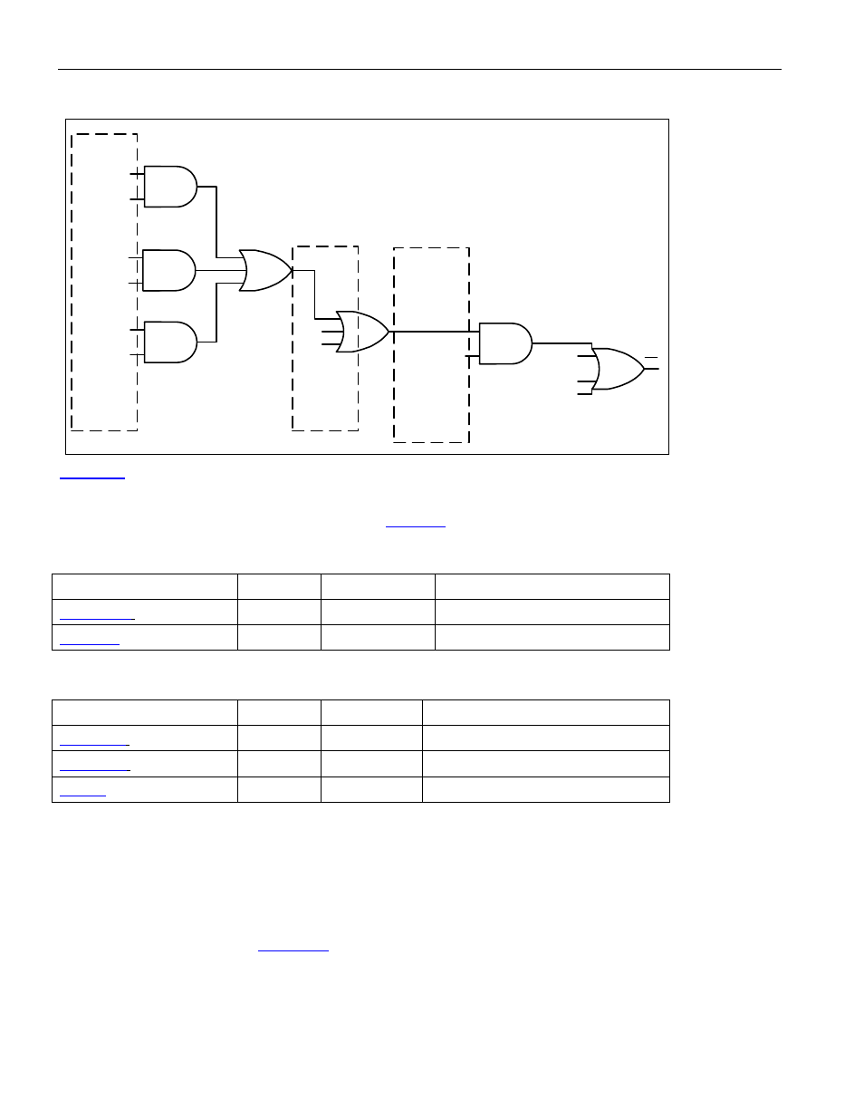
Figure 9-1. Interrupt Structure
GL.ISR.PISRn
PORT.ISR bit
SRL bit
SRL bit
SRL bit
SRIE bit
SRIE bit
SRIE bit
BLOCK LATCHED
STATUS and
INTERRUPT
ENABLE
REGISTERS
PORT INTERRUPT
STATUS
REGISTER
GLOBAL
INTERRUPT
STATUS REGISTER
and INTERRUPT
ENABLE REGISTER
GL.ISRIE.
PISRIEn
INT
PORT
INTERRUPTS
GLOBAL
INTERRUPTS
not only tells the user how to determine which event caused the interrupt, it also tells the user how to
enable a particular interrupt. Each block has a Status Register Interrupt Enable register which must be set in order
to enable an interrupt. The next step is to unmask the interrupt at the port level. This is controlled in the Global
Interrupt Status Register Interrupt Enable register (
). Now the device is ready to drive the INT pin low
when a particular status bit gets set.
For example, in order to enable DS3 Out of Frame interrupts, the following registers would need to be written:
Register bit
Address
Value Written
Note
.OOFIE
0x12C
0x0002
Unmask OOF interrupt
.PISRIE
0x012
0x0010
Unmask Port interrupts
The following status registers bits will be set upon reception of OOF:
Register bit
Address
Value Read
Note
.OOFL
0x128
0x0002
DS3 Out of Frame
.FMSR
0x050
0x0001
Framer Block Interrupt Active
.PISR
0x010
0x0010
Port Interrupt Active
9.2 Clocks
9.2.1 Line
Clock
Modes
9.2.1.1 Loop Timing Enabled
When loop timing is enabled (
.LOOPT), the transmit clock source is the same as the receive clock
source. The TCLKI pin is not used as a clock source. Because loop timing is enabled, the loopback functions (LLB,
PLB and DLB) do not cause the clock sources to switch when they are activated. The transmit and receive signal
pins can be timed to a single clock reference without concern about having the clock source change during
loopbacks.