Figure 7-33. clear status latched register on read, Figure 7-33, Figure 7-34 – Rainbow Electronics DS3170 User Manual
Page 49
DS3170 DS3/E3 Single-Chip Transceiver
49 of 233
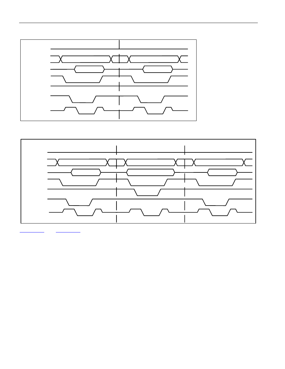
Figure 7-33. Clear Status Latched Register on Read
D[15:0]
A[10:1]
A[0]/BSWAP
0x1C0
0xFFFF
0x1C0
0x0000
Z
Z
Z
Z
RD
WR
CS
RDY
Figure 7-34. Clear Status Latched Register on Write
D[15:0]
A[10:1]
A[0]/BSWAP
0x1C0
0xFFFF
0x1C0
0x5555
0x1C0
0xAAAA
Z
Z
Z
Z
Z
Z
RD
WR
CS
RDY
and
show exaggerated views of the Ready Signal to describe the difference in access
times to write or read to or from various memory locations on the DS3170 device. Some registers will have a faster
access time than others and if needed, the user can implement the RDY signal to maximize efficiency of read and
write accesses.
See also other documents in the category Rainbow Electronics Communication:
- MAX12005 (14 pages)
- MAX7058 (14 pages)
- MAX9995 (13 pages)
- MAX7034 (13 pages)
- MAX7033 (16 pages)
- MAX9476 (8 pages)
- MAX9486 (8 pages)
- MAX14821 (29 pages)
- MAX9489 (11 pages)
- MAX9491 (11 pages)
- DS2130Q (22 pages)
- DS21458 (270 pages)
- DS3131 (174 pages)
- DS26502 (125 pages)
- DS2153Q (48 pages)
- DS26503 (123 pages)
- DS2186 (11 pages)
- DS1842A (6 pages)
- DS3134 (203 pages)
- DS1876 (69 pages)
- DS1874 (88 pages)
- DS31256 (181 pages)
- DS2141A (35 pages)
- DS3184 (13 pages)
- DS2154 (69 pages)
- DS26504 (128 pages)
- DS3164 (12 pages)
- DS1852 (25 pages)
- DS2181A (32 pages)
- DS2151Q (46 pages)
- DS1843 (8 pages)
- DS2165Q (17 pages)
- DS2180A (36 pages)
- DS2172 (20 pages)
- DS2152 (79 pages)
- DS1841 (16 pages)
- DS2182A (22 pages)
- DS2143Q (40 pages)
- DS2132A_Q (17 pages)
- DS1862 (42 pages)
- DS26519 (310 pages)
- DS2188 (11 pages)
- DS1875 (92 pages)
- DS33M33 (20 pages)