Jtag functional timing, Io pins, Jtag f – Rainbow Electronics DS3170 User Manual
Page 207: Unctional, Iming, Io p, Figure 12-3. jtag functional timing, 5 jtag functional timing, 6 io pins
DS3170 DS3/E3 Single-Chip Transceiver
207 of 233
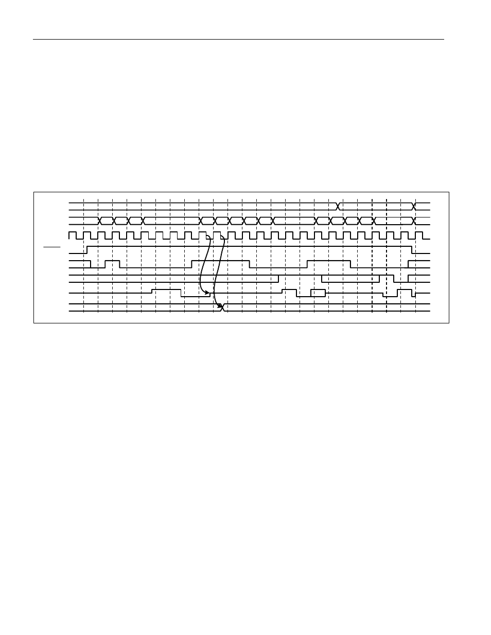
12.5 JTAG Functional Timing
This functional timing for the JTAG circuits shows:
· The JTAG controller starting from reset state
· Shifting out the first 4 LSB bits of the IDCODE
· Shifting in the BYPASS instruction (111) while shifting out the mandatory X01 pattern
· Shifting the TDI pin to the TDO pin through the bypass shift register
· An asynchronous reset occurs while shifting
Figure 12-3. JTAG Functional Timing
JTCLK
JTRST
JTMS
JTDI
JTDO
(STATE)
Reset
X
Run Test
Idle
Select DR
Scan
Capture
DR
Shift
DR
Exit1
DR
Update
DR
Select DR
Scan
Select IR
Scan
Capture
IR
Shift IR
Exit1
IR
Update
IR
Select DR
Scan
Capture
DR
Shift
DR
Test
Logic Idle
(INST)
IDCODE
BYPASS
IDCODE
X
X
X
X
X
Output
Pin
Output pin level change if in "EXTEST" instruction mode
12.6 IO Pins
All input, output, and inout pins are inout pins in JTAG mode.