Rainbow Electronics MAX9486 User Manual
General description, Applications, Features
General Description
The MAX9486 low-cost, high-performance clock syn-
thesizer with an 8kHz input reference clock provides six
buffered LVTTL clock outputs at 35.328MHz. The clock
synthesizer can be used to generate the clocks for T1,
E1, T3, E3, and xDSL.
The MAX9486 has two phase-lock loops (PLLs). The
first PLL uses a voltage-controlled crystal oscillator
(VCXO). The second PLL is a frequency multiplier. With
the two PLLs, the MAX9486 generates the output fre-
quency at 35.328MHz. In addition, this device gener-
ates a jitter-suppressed 8kHz output that provides a
better source for the reference clock relay.
The MAX9486 is available in a 24-pin TSSOP package
and operates over the extended operating temperature
range of -40
°C to +85°C and a single +3V to +3.6V
power-supply range.
Applications
Telecom Equipment Using T1, E1, T3, E3, and
ISDN Protocols
xDSL Equipment in CO with Interface to the
Telecom Protocols
Features
♦ 8kHz Input Reference CLK
♦ High-Jitter Rejection on the Reference CLK
♦ Synthesizer Locks to the 8kHz Reference with a
±200ppm Range
♦ Output Frequency: 35.328MHz
♦ Six Buffered LVTTL Low-Jitter Outputs
♦ One 8kHz Reference CLK Relay Output
♦ +3.3V Supply Operation
♦ 24-Pin TSSOP Package
MAX9486
8kHz Reference Clock Synthesizer
with Multiple Outputs at 35.328MHz
________________________________________________________________ Maxim Integrated Products
1
Ordering Information
19-3345; Rev 0; 8/04
For pricing, delivery, and ordering information, please contact Maxim/Dallas Direct! at
1-888-629-4642, or visit Maxim’s website at www.maxim-ic.com.
EVALUATION KIT
AVAILABLE
PART
TEMP RANGE
PIN-PACKAGE
MAX9486EUG
-40
°C to +85°C
24 TSSOP
24
23
22
21
20
19
18
17
1
2
3
4
5
6
7
8
CLK1
GND
CLK2
V
DD
V
DDP
REIN
REO
TOP VIEW
CLK3
V
DD
GND
CLK4
X2
V
DD
X1
GNDP
16
15
14
13
9
10
11
12
V
DD
CLK5
GND
CLK6
SETI
LP1
LP2
GND
TSSOP
MAX9486
SHDN
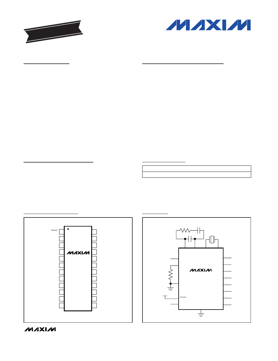
Pin Configuration
MAX9486
CLK2
X1
CLK1
V
DDP
GNDP
X2
REO
CLK6
CLK5
CLK4
CLK3
GND
V
DD
LP1
LP2
REIN
R
SET
R
1
C
1
C
2
SETI
V
DD
SHDN
Typical Application Circuit