2 calculating input data (a/d), Kv -300 – KEYENCE Visual KV Series User Manual
Page 345

8.4 Programming
KV-300 Series Only
KV
-300
KV-10/80
Chapter 8 KV-AN6 Analog I/O Module
1-321
1
8
Full scale and resolution of each range
(12-bit BIN data)
Negative input data is treated as a 2’s complement.
•
Maximum value (+10 V, +5 V, 20 mA)
•
Minimum value (-10 V, -5 V, 0 mA)
(4 mA)
8.4.2
Calculating Input Data (A/D)
The KV-AN6 converts analog input signals to 16-bit digital values and writes them
into data memory. (The effective bits are the 12 bits starting from the most signifi-
cant digit.)
This section describes how to convert the data stored in data memory into digital
data (in decimal) according to the input range.
•
Full scale and resolution of each range
The following table shows the full scale and resolution of each range.
•
Since the effective bits that are written into data memory are the 12 bits starting
from the most significant digit, resolution is 1/4000 of the full-scale value.
To calculate the input voltage value or input current value from the data written
into data memory, use the following expressions:
Input voltage = DM value/16 x Resolution of the input range
Input current = (32000 + DM value)/16 x Resolution of the input range
To convert a 16-bit DM value to an effective 12-bit value, divide the 16-bit value
by 16.
Example 1
When 19200 (in decimal) is written into DM addresses in the ±10 V range
19200/16 x 5 mV = 6000 mV = 6 V
The KV-AN6 receives input of +6 V.
Example 2
When 12800 (in decimal) is written into DM addresses in the ±5 V range
12800/16 x 2.5 mV = 2000 mV = 2 V
The KV-AN6 receives input of 2 V.
Example 3
When 16000 (in decimal) is stored in DM addresses in the 0-to-20 mA range
(32000 + 16000)/16 x 5 µA = 15000 µA = 15 mA
The KV-AN6 receives input of +15 mA.
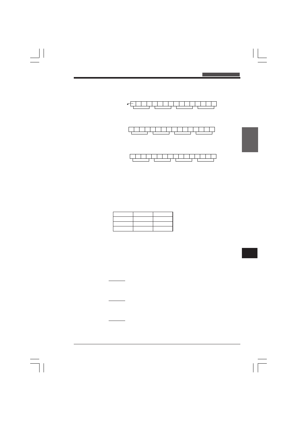
D15 D14 D13 D12 D11 D10 D09 D08 D07 D06 D05 D04 D03 D02 D01 D00
0
0
0
0
Sign bit
0: Positive
1: Negative
Hexadecimal
Hexadecimal
Hexadecimal
Undefined
Data memory
addresses
Undefined
D15 D14 D13 D12 D11 D10 D09 D08 D07 D06 D05 D04 D03 D02 D01 D00
0
1
1
1
1
1
0
1
0
0
0
0
X
X
X
X
7
D
0
Undefined
D15 D14 D13 D12 D11 D10 D09 D08 D07 D06 D05 D04 D03 D02 D01 D00
1
0
0
0
0
0
1
1
0
0
0
0
X
X
X
X
8
3
0
Range
Full scale
Resolution
±10 V
20 V
5 mV
±5 V
10 V
2.5 mV
0 to 20 mA
20 mA
5 µA
KVHKA Chap 08.p65
08.3.11, 11:19 AM
321
