5 about the register address tables – Zilog Z16C30 User Manual
Page 36
2-10
Z16C30 USC
®
U
SER
'
S
M
ANUAL
UM97USC0100
Z
ILOG
2.9.5 About the Register Address Tables
Tables 2-1 and 2-2 show the names and addresses of the
addressable registers in the USC, in address and alpha-
betical order. The Tables assume that SRightA (BCR0) is
1. The RegAddr column in the Tables reflects the state of
AD5-AD1, AD13-AD9, or CCAR5-1 as applicable.
If “16-bit” (BCR2) is 1, the B//W bit from AD6, AD14, or
CCAR6 selects between a 16-bit transfer (if 0/low) and an
8-bit transfer (if 1). If “16-bit” is 0, the USC ignores AD6,
AD14, or CCAR6 (as applicable). Note that the values in
the “8-bit data” columns of Tables 2-1 and 2-2 include the
B//W bit 1 for both direct and indirect addressing, as is
required on a 16-bit bus. When 16-bit (BCR2) is 0 these
address values can be used as shown, or 64 lower like the
addresses shown in the “16-bit data” columns.
For 8-bit transfers on either an 8- or 16-bit bus, the state of
AD0, AD8, or CCAR0 selects the less-significant 8 bits of
the register (if 0/low) or the more-significant 8 bits if 1/high.
In this regard the USC is “little Endian” like Intel micropro-
cessors. For 16-bit transfers, AD0, AD8, or CCAR0 must be
0/low.
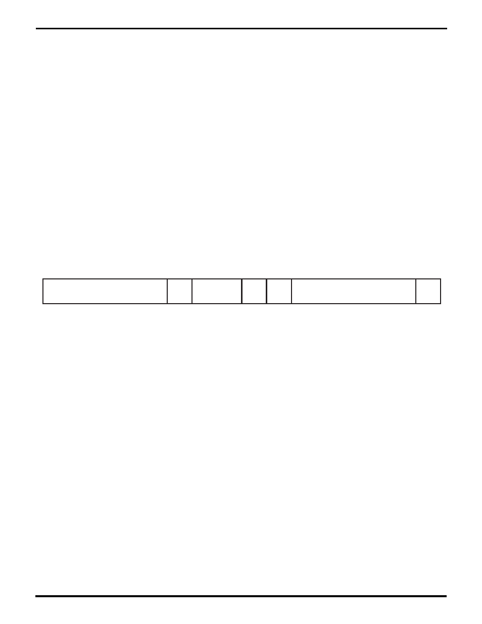
RegAddr
RTMode
Chan
Load
U//L
RTCmd
B//W
14
13
12
11
10
9
8
7
6
5
4
3
2
1
0
15
RT
Reset
Figure 2-8. The Channel Command/Address Register (CCAR)
The Direct Address columns of the Tables assume:
(1) SRightA (BCR0) is 1,
(2) the processor’s multiplexed AD6-AD0 lines are con-
nected to AD6-AD0, or its A5-A0 lines are connected
to AD13-AD8, depending on SepAd (BCR15),
(3) the D//C pin is grounded, and
(4) the processor’s A7 line is connected to A//B.
If your design differs from these assumptions, register
addressing will be different from that shown in the Direct
Address columns.
UM009402-0201