Zilog Z16C30 User Manual
Page 175
8-20
Z16C30 USC
®
U
SER
'
S
M
ANUAL
Z
ILOG
UM97USC0100
14
13
12
11
10
9
8
7
6
5
4
3
2
1
0
15
CTR0Div
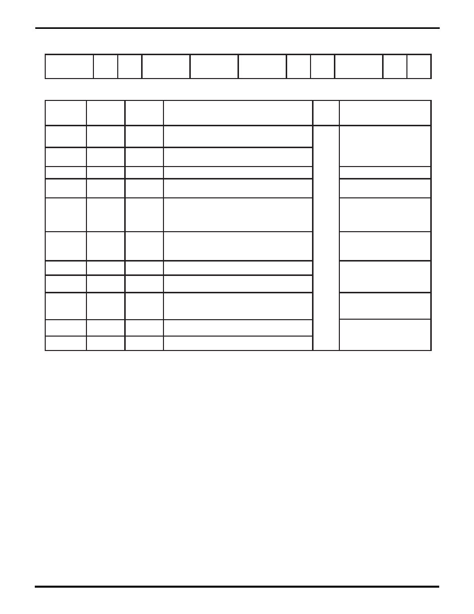
Hardware Configuration Register (HCR)
Register Address 0 b 01001
Bit(s)
Field/Bit
Name
Conditions
/Context
Description
RW
Status
Ref Chapter: Section
TxAMode
HCR15-14
CTR1
DSel
DPLLMode
00=CTR0 divides by 32;
01/16; 10=/8; 11=/4
RW
4: Tx and Rx Clocking
CTR0 and CTR1
CVOK
DPLLDiv
BRG1S BRG1E
RxAMode
BRG0S BRG0E
CTR0Div
HCR13
0=CTR0Div determines CTR1 divisor;
1=DPLLDiv determines CTR1 divisor
CTR1DSel
HCR12
1=don't report single code violations
CVOK
Biphase
4: More About the DPLL
HCR11-10
00=DPLL divides by 32; 01=/16; 10=/8;
11=do not use for DPLL (/4 for CTR1)
DPLLDiv
4: Tx and Rx Clocking;
Introduction to the DPLL
HCR9-8
00=disable DPLL;
01=run DPLL for NRZ modes;
10=run DPLL for Biphase-Mark or -Space;
11=run DPLL for either Biphase-Level mode
DPLLMode
4: The /TxACK and /RxACK
Pins
HCR5
1=BRG1 single cycle mode; 0=continuous
BRG1S
4: Tx and Rx Clocking
The Baud Rate Generators
HCR4
1=enable BRG1
BRG1E
HCR1
1=BRG0 single cycle mode; 0=continuous
BRG0S
HCR0
1=enable BRG0
BRG0E
HCR7-6
TxAMode
00=/TxACK pin is a general-purpose input;
01=/TxACK is a Tx DMA Acknowledge input;
10=drive /TxACK Low; 11=drive /TxACK High
4: More About the DPLL
HCR3-2
RxAMode
00=/RxACK pin is a general-purpose input;
01=/RxACK is a Rx DMA Acknowledge input;
10=drive /RxACK Low; 11=drive /RxACK High
4: The /TxACK and /RxACK
Pins
4: Tx and Rx Clocking
The Baud Rate Generators
RW = Read/Write, RO = Read Only, WO = Write Only – for other codes see p. 8-10.
UM009402-0201